
Undergraduate Thesis Research
Instructor: Prof. Yaqing Bie from Sun Yat-sen University
Duration: 08/2020-08/2021
Abstract
Phonon vibration modes are closely related to lattice structure, symmetry, defects and deviations. Twisted 2D materials(2DMs) can activate more Raman-inactive vibration modes. Therefore, an in-depth Raman spectroscopy research on twisted 2DMs is necessary to fully understand the properties of the materials. Moreover, the superlattice introduced by the twisted 2DMs causes the appearance of Moiré phonons,which means that Moiré have a modulating effect on phonon transport. Raman spectroscopy is the relatively simplest method to characterise this modulating effect. However, not all material systems have been studied in detail for their phonon vibration modes, and the physical mechanisms of Moiré phonons vibration have not been fully and comprehensively discussed, due to limitations in preparation techniques and experimental progress.
This project has developed the following stable preparation process for materials where large area mechanical desorption is difficult to achieve: mechanical cleavage, followed by atomic force microscope cutting and dry transfer. This method is used for most 2D Materials that can be mechanically cleavage and allows the preparation of twisted 2D Materials samples with relatively small area. It could facilitate the Raman study of twistronics. What is more, this method does not require the aid of other 2D materials, allowing better study of the phonon vibration modes of the material itself.
In this project, three twisted qualayer molybdenum telluride(MoTe2) with different rotation angles were successfully fabricated by using this process. The project also involved the measurement and analysis of the prepared samples by Raman spectroscopy, which led to the following conclusions: the degree of relative twisted angle is closely related to the Raman-shift of $A_1g$ and $B^1_{2g}$ mode.The relative rotation degree could be judged by Raman-shift of the peaks. According to the symmetry of the atomic arrangement and the data analysis, this paper predicts that the Raman-shift of these peaks will be exhibiting barely a"V-shape"behavior with the 30° as the symmetry axis within the twisted range of 1° to 59° . However, the current research results failed to find the new rise of vibration modes from moiré phonons.In response to the failure of observing Moiré phonon vibration modes, this paper also proposes improvements to both the preparation and measurement experiments. The results of the present tentative experiments are also shown in this paper. It is hoped that through these methodological improvements, it may be possible to observe the emergence of Moiré phonon vibrational modes and gain insight into the role the Moiré pattern plays in the modulation of phonons.
By studying all the vibrational modes of the material, it is possible to gain a better understanding of the properties of this material and to provide information for the future devices fabrication. In addition, the study of the Moiré phonon vibration modes provides a clear understanding of the physical mechanisms. The ability of the Moiré pattern to modulate phonon transportation and the physical mechanism, helps develop the ”phonon engineering” and provides the possibility to prepare more outstanding performance devices.
Keywords: Atomic Force Microscope Cutting; Raman Spectroscopy; Interlayer Phonon Vibration Mode; Moiré Phonon; Twisted Qualayer MoTe2
Chapter 1: Introduction
Two-dimentional materials (2D Materials) refer to crystalline solids consisting of a single layer of atoms. Since these materials have one less dimension than bulk materials, the excellent mechanical, optical, and electrical properties of 2D materials are far superior to those of bulk materials. Based on the excellent properties of 2D materials, the devices designed based on them also have excellent performance, with broad application prospects. 2D Materials are currently one of the hottest interests in academic research. 2D materials have a huge family of materials, and MoTe2 is one of them. This project mainly focuses on the Raman study of a special 2D material - Molybdenum Ditelluride (MoTe2), and its twisted samples.
In this chapter, background, related work and research importance have been detaily explained.
Background
In 1965, Gordon Moore Gave a famous speech mentioning Moore’s Law, which became a prediction for the semiconductor industry. [1] However, as the device size continues to shrink, new physical problems brought by the small size also rise. “Heat death” and “quantum uncertainty” are two main problems. New devices based on new materials have become one of the important ways to solve the problem. Among them, 2D materials are one of the hottest research topics.
Since the discovery of graphene in 2004 by Professor Jem and Professor Novoselov of the University of Manchester [2] , more 2D materials have been discovered and studied by scientists, and great progress has been made. According to the elemental composition, materials can be mainly divided into the graphene family, Xenes, chalcogenides, 2D oxides and Transition Metal Dichalcogenides (TMDCs).
Since 2D materials have no interlayer interactions, single-layer or thin-layer 2D materials have less electronic confinement and have excellent electrical properties. At the same time, since the thickness of 2D materials is at the atomic level, which provides great mechanical flexibility and optical transparency, it is expected to become a new generation of optoelectronic devices for fabrication of high flexibility and transparency. Based on the excellent mechanical, optical, and electrical properties of 2D materials, the heterostructures by stacking different 2D materials can be applied to field effect transistors, diodes and other applications. [3] These applications may help solve problems encountered in bulk material-based devices. However, due to the huge family of 2D materials, different 2D materials-based structural characterizations and studies are not very detailed and thorough.
Among these structures, a special heterostructure, the twisted structure, has made great progress in recent years and has attained high attention. The twisted structure is to replace the other 2D materials of the heterojunction with the same 2D material, and form different atomic arrangements through relative rotation, thereby changing the arrangement of atoms between different layers to form a heterostructure. The superlattice is formed because the upper and lower layers interact with each other due to the twisted mismatch of the two layers. In the superlattice, the physical properties of the material will change, and the energy band, transport properties and other properties can be regulated by controlling the degree of the relative angle. At the same time, the formation of moiré patterns and superlattices from the twisted structure introduces new physical properties, which have attracted the attention of researchers. There are several ways to characterize the twisted structure: Raman spectroscopy, photoluminescence spectroscopy, second harmonic research, and light absorption research. As a means to directly study the phonon-related properties of the material itself, Raman spectroscopy can reflect the crystal structure, symmetry, defects and impurities of the material itself. The characterization of the results of twisted 2D materials can enrich more phonon vibration modes, which is of great significance for understanding the properties of the materials themselves.
Although the properties of the twisted structure of some materials such as graphene and twisted molybdenum sulfide have been fully studied, the studies in the twisted 2D materials which cannot be obtained by growth methods and obtained with small area by mechanical cleavage are still incomplete. Limited by the single layer preparation method, the development of a small-area-friendly 2D material twisted preparation method is particularly important in the sustainable development of the twisted structure. The focus of this project has developed a process that can relatively stably prepare small-area 2D twisted samples. The structure is characterized by Raman Spectroscopy, and its phonon mode is studied, so as to fully understand the influence of the twisted stacking on the atomic lattice. The Moiré pattern is also studied in its effect on the phonon and its vibration modes.
Based on the study of the phonon vibration modes under the twisted structure, we can understand the effect of Moiré patterns on phonons while better understanding this material. According to the relevant work, the phonon transport capacity under the superlattice will be improved. By using this method to prepare more 2D twisted structures, it is beneficial to understand the regulation of Moiré patterns on phonon transport under the same material system or under different material systems. Based on the generation of Moiré patterns and the physical mechanism, it is possible to develop "phonon engineering" because it might help solve the "heat depth" problem by controlling the carrier of heat - phonon.
Related Work
The development of twisted structure
This section briefly reviews and summarizes the development history of twisted structure research and the physical phenomena under beneath. Then, this section will focus on the 2D materials that are currently more deeply studied by Raman spectroscopy, starting with twisted graphene, and representative materials of twisted TMDCs. . The development status of MoS2 and other 2D material systems is summarized.
The earliest research began with twisted graphene. The researchers found that the atoms in the upper and lower layers of naturally occurring or artificially synthesized highly oriented pyrolytic graphite usually undergo dislocation and rotation to form a superlattice [4;5] . Scientists began to think about whether the appearance of superlattices and changes in the stacking method would have an impact on the energy bands of graphene, and conducted theoretical and experimental studies. However, the area of the relative angle is very small at this time, which restricts the study of Moiré patterns to be observed only by scanning tunneling microscopy without looking into optical properties and mechanical properties.
With the development of twisted preparation technology, the area of the twisted structure is getting larger and larger, making more characterization methods possible. At the same time, advances in characterization methods have also enabled more material information to be observed. For example, the researchers proposed that the Moiré patterns will generate a periodic potential, which can enable electrons to interact with each other, resulting in various special physical phenomena with excellent performance. This idea is based on the experimental observation that twisted bilayer graphene produces a Moiré flat band due to its extremely strong interlayer coupling, and the velocity on Dirac point passes through zero several times as the twisted decreases [6] . This phenomenon fully illustrates the electrical regulation of Moiré patterns. According to the latest research results, twisted three-layer twisted graphene has stronger electronic structure tunability and superconductivity than double-layer graphene, and the existence of this superconductivity and superlattice simultaneously appear as two current carriers It is caused by the phase of the broken symmetry, which is confined to the van der Waals singularity. The findings also suggest that twisted trilayer twisted graphene can be electrically tuned to move closer to the Bose-Einstein condensation, or break the understanding of strongly coupled superconductivity. [7]
The development of preparation and characterization technology has made the research materials no longer limited to twisted graphene, and the main topic is not only focused on electrical properties, but also optical properties. For direct bandgap semiconductor TMDCs with strong light-matter interaction, the twisted structure of the TMDCs also produces moiré potential, which produces moiré excitons in optical properties. [8] Based on the Raman-inactive hexagonal boron nitride can be excited through the interlayer coupling of the heterostructure composed of tungsten selenide and hexagonal boron nitride, the Raman peak activity is speculated. [9] This led the researchers to question whether this activation also exists in the twisted structure.
Compared with the heterostructures composed of 2D materials with different lattice sizes, the lattice structure of the twisted bilayer has greater periodic symmetry, and the period of its crystal superlattice depends on the relative rotation angle. Due to the phonon folding effect of the superlattice, the folded acoustic and optical phonons should be observed by Raman spectroscopy. At the same time, the interlayer coupling in the twisted-structured superlattice also induces a periodic potential that can generate additional phonons, which can be understood by Raman spectroscopy. The twisted bilayer structure is the simplest prototype to understand the basic properties of the heterostructure, so the Raman characterization and research of the twisted structure are of great significance. [10] At the same time, Raman characterization is beneficial to understand the crystal structure, symmetry, defects and impurities of the material itself, so as to further understand the properties of the material itself. It's also beneficial to apply to different applications based on it.
In addition to Raman spectroscopy, optical absorption, photoluminescence (PL), and Second Harmonic Generation (SHG) measurements are also commonly used to characterize optical properties. According to the literature, the controllable twisted graphene light absorption compared with Bernal stack/AB stacked bilayer graphene, the efficiency of light absorption is about 35%, from the original 4.6% to about 6.2%. [11] According to a study in 2014, in the PL spectra of the twisted molybdenum sulfide samples, the PL peaks associated with the electronic coupling within the layer vary greatly under the modulation of the twisted angle. Although the research progresses on the twisted structure in 2019, a new physical concept - moiré exciton rises. This is closely related to the Moiré potential mentioned above, which affects the electronic coupling within the layer. [12] At present, the research on light absorption, PL spectrum, and SHG is still studied.
Development of Twisted Graphene
According to the current study, twisted graphene belongs to the system of bilayer breathing mode. Since the superlattice exhibits a θ-dependent orientation, a new long acoustic branch is excited in the Brillouin zone, which can be measured by first-order Raman scattering. It is worth noting that there are some similarities and differences between the first-order Raman measurement and the second-order Raman measurement.
According to the Raman measurement of different twisted bilayer graphene, as shown in Figure 1.1., the formation of a superlattice will cause the following R peaks in the Raman measurement, which are highlighted with "*" in the figure. Curves with different colors represent excitation light at different wavelengths. Red, green, and blue represent: 633 nm, 514 nm, and 488 nm, respectively. Black is the peak position of silicon itself. By observing these new R peaks, it can be concluded that the superlattice activates the phonons inside the Brillouin zone, and the relative rotation angle θ will determine the wave vector, enabling modulation. Different vibrational peaks correspond to different phonon branches. [13]
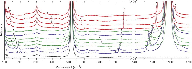
Fig 1.1 - First-order Raman spectroscopy of twisted graphene [13]
For second-order Raman systems, the 2D peak (G' peak) can only be activated if there are defects in the graphene system. Its frequency depends on the excitation light wavelength, and is very sensitive to changes in the band structure of electrons and phonons, so the vibrational mode characterization of twisted graphene can be carried out through this vibrational mode. [14] According to Kim's research, the Full width at half maximum(FWHM), center wavelength of the 2D peaks all change with θ, as shown in Figure 1-2. [15]
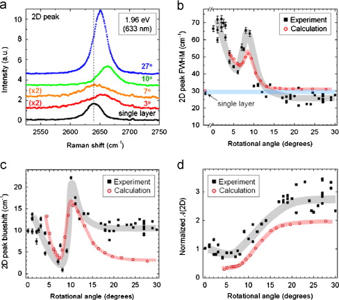
Fig 1.2 - Second-order Raman Spectroscopy of twisted graphene [15]
The researchers also studied the double vibration modes of the twisted graphene, and came to the following conclusions: (1)the phonons in the valley are concentrated at the Γ point, while the phonon of double resonance outside the valley is near the K point;(2)the wave vectors of the different phonons of the double resonance Raman both are concentrated at the Γ point and K point of high symmetry; (3)under different excitation energies of light, the wave vector of the double resonance will change;(4)under the double resonance Raman, the defect peak needs to be activated to appear. [16]
In the latest twisted Raman research, the researchers based on the principle that the electronic energy level structure of twisted graphene can achieve a low-energy Van Hove singularity through layer coupling. By adjusting the stacking angle of the twisted graphene, thereby modulating the third-order optical nonlinearity. Third-Harmonic Generation (THG) efficiency is greatly improved when the energy gap of the van Hove singularity matches the three-phonon resonance frequency of the incident light. Compared with the modulation of single-layer graphene, the efficiency of gate-controlled THG is enhanced by 60 times, and it has broad application prospects in tunable nonlinear optical devices. [17]
Phonon mode study of twisted molybdenum sulfide(MoS2)
For twisted 2D materials, due to the phonon folding effect of the superlattice, Raman spectroscopy can observe the positions of the acoustic branch and the optical branch after folding. The appearance of a superlattice also introduces a Moiré potential to the interactions within the layers. According to the study of the twisted MoS2 by the Pingheng Tan's group, since this potential is not strong enough to form a new lattice-matched structure, the two wave vectors of the monolayer molybdenum sulfide will fold to the regional center Γ in the Moiré inverted space point. These phonons will become Raman active and new vibrational modes will appear. According to the symmetry of the atomic crystal arrangement, the Raman frequency shift center position change curve of these folded peaks should be a "V"-shaped curve with 30° as the symmetry axis. But it is worth noting that the coupling of the shear modes in the layers is not enough to make new changes in the shear modes in the layers. At the same time, in order to distinguish the new mode caused by Moiré phonons from the peaks related to the second-order Raman, the study also characterized the samples using Raman systems with different wavelengths, and found that when the excitation wavelength is close to the C excitons, the Moiré sound The intensity of the sub-correlated vibrational modes will be greatly improved. This fully demonstrates that the excitation of the Moiré phonon vibrational mode is generated by the exciton effect.
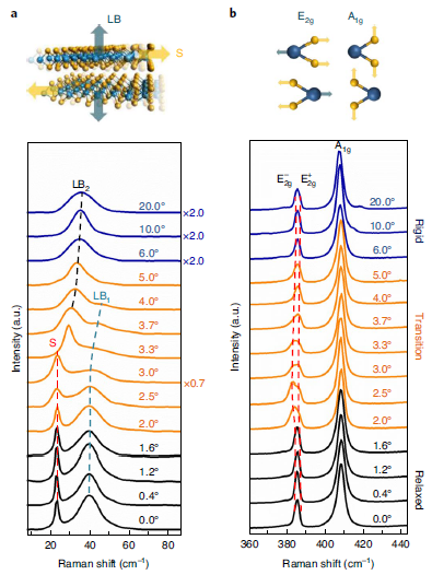
Fig 1.3 -Twisted MoS2 Raman spectroscopy [18]
The latest research on twisted MoS2 has investigated small angles, whose Raman spectra are shown in Figures 1.3. According to the difference of Raman spectra, it can be divided into three regions: Relaxed Regime (0◦ ≤ θ < 2◦), Rigid Regime (θ ≥6◦) and Tradition Regime (2◦ ≤ θ < 6◦). Based on the symmetry, researchers speculate that these regions, phonons, will be renormalized. Near-field scanning presents challenges for the limitations of current scanning tunneling microscopy techniques. Then in the transition region, Raman spectroscopy can observe continuous, faint changes in atomic configuration and strain. This provides a new method for the study of material properties. [18]
Phonon Vibratoin Mode of other twisted 2D materials Research
In addition to the two materials mentioned above, the research on the twisted structure of 2D materials such as tungsten selenide(WSn), tin diselenide(SnSe2), and tungsten disulfide(WS2) is the research object. According to the new study, low wavenumber measurements of twisted WSn can be used as a criterion for judging favorable relative angles of twisted samples. The central wavelength of the breathing mode shifts significantly with the change of angle. Its moving trend also takes 30° as the axis of symmetry, forming a symmetrical curve. In the range of 5° to 7°, the interlayer breathing pattern changes showed a clear angular dependence. But the blue-shift of the breathing mode only lasted to ∼14°, while the Raman frequency shift of the post-breathing mode remained almost unchanged. [19]
Reserch proposal and importance
Raman spectroscopy is a powerful characterization method for the study of phonon vibrational modes in 2D materials. Although some 2D materials, such as graphene, MoS2 and other twisted structures have gradually deepened, the physical mechanism for the generation of "Moiré phonons" has not yet been unified. Therefore, it is necessary to study and discuss different material systems and unify their related physical mechanisms. For some 2D materials that are difficult to grow a single layer, the Raman research is still in its infancy, and MoTe2 is one of the 2D materials.
Compared with well-grown 2D materials such as sulfide and selenide, the atomic mass of the tellurium atom in MoTe2 is larger, and the phonon vibration mode is quite different from it. In order to understand all the phonon vibrational modes of MoTe2 and the Moiré phonons associated with MoTe2, a Raman study was performed on twisted MoTe2. In the selection of the number of MoTe2 layers, because the single-layer MoTe2 is easily oxidized at high temperature, and the transfer process needs to experience high temperature, this project selects a relatively stable and photoelectric property comparable to the single-layer MoTe2. Double-layer MoTe2 was used as the research object.
The monolayer or thin layer of MoTe2 can only be obtained by mechanical cleavage, but due to its crystal size limitation and strong interlayer interaction, the obtained monolayer 2D material has only one side or only one side. ten microns. Its thin layer size greatly limits the fabrication of twisted structures, posing challenges to the continued development of twisted structures.
Aiming at this situation, this paper develops a method for the preparation of small-area twisted 2D structure samples through mechanical cleavage, which is friendly to experiments where the upper and lower cladding layers interfere with the measurement. This method includes three processes: mechanical cleavage, atomic force microscope cutting, and dry transfer. These three processes and other methods are discussed in depth in this paper. With this method, the project prepared three twisted MoTe2 samples and carried out Raman spectroscopy measurement and data analysis. Through the characterization of the twisted samples, we can understand the phonon vibration mode of the twisted MoTe2, and better understand its crystal structure, symmetry and other material properties. This method is effective for most twisted sample preparations where thin layers can be obtained by mechanical cleavage.
In the follow-up experiments, based on the reflection on the measurement results, this project also conducted a tentative experiment to improve the experiment. In this paper, in addition to non-damaging and localized surface cleaning methods for 2D materials, an atomic force microscopy method for enhancing interlayer interactions and a thermal annealing method are proposed. Through these methods, the quality of the prepared twisted samples is continuously improved to better and comprehensively study the phonon vibration modes of the twisted samples.
Chapter 2: Twisted MoTe2 Fabrication Process
Since the beginning of twisted research, the sample preparation of twisted 2D material has mainly been through the growth of twisted 2D material structures, or assisted by other 2D materials. The development of this project is aimed at the twisted preparation method of small-area 2D materials that can only be prepared by mechanical cleavage without the assistance of other 2D materials. In the first section of this chapter, the paper introduces the mechanical cleavage, and briefly explains and compares it with other methods. The second section explains the AFM cutting method in detail. Using this cutting method, the same thin-layer sample can be cut into two parts while retaining a larger area of the sample without other 2D materials assistance. The principle, process and cutting effect will be shown in this section. Other commonly used cutting methods will also be described. The advantages and disadvantages of each method will be compared and analyzed. Dry transfer is the final step in the preparation of the twisted sample structure in this project and will be described in detail in the third session of this chapter. By dry transfer, the cut samples are stacked into twisted structure samples to complete the preparation of the twisted structure. The principle, process and preparation results of dry transfer will be demonstrated in this section. In addition, other transfer methods will also be briefly summarized in this section.
Monolayer Exfoliation
In order to prepare the twisted samples, obtaining a thin layer sample is the first step of the experiment. In this section, various ways to obtain thin layers of 2D materials will be introduced, and the mechanical cleavage method used in this project will be described in detail.
Related ultra-thin layer fabrication techniques
There are a variety of techniques to obtain ultra-thin layers, including cleavage, liquid exfoliation, ion intercalation exfoliation, chemical vapor deposition, wet chemical synthesis. [3]
The earliest and common method for preparing thin layers of 2D materials started from mechanical cleavage. It utilizes that the interaction between the adhesive tape and the 2D material is greater than the interlayer van der Waals force between the 2D materials to achieve thinning, and finally the sheet is transferred to the target substrate. This method can obtain relatively high-quality samples, but the yield is relatively low and extremely random. [2] Liquid exfoliation is also a traditional method. Ultra-thin sample is attained by using ultrasound by placing the bulk crystals in Dimethylfor-Mamide (DMF) or N-Methyl-Pyrrolidone (NMP). This method utilizes the ultrasonic energy to destroy the van der Waals forces between the layers to achieve thinning of the material. This method enables relatively low-cost, high-yield fabrication of ultrathin 2D materials, but due to the toxicity of these organic solvents, there are high requirement for production equipment. Meantime, these organic solvents will remain on the 2D material, affecting the properties of the subsequent preparation of the 2D material device. [20]
The ion exfoliation method is to obtain thin-layer samples by embedding organic metal compounds in the interlayer space of bulk crystals to reduce the interlayer interaction force. This approach enables precise control of ion intercalation for efficient thinning. However, since the experimental process needs to last for a long time at high temperature, and the organometallic compounds may explode if exposed to oxygen and water, the preparation process is relatively cumbersome. [21]
Chemical vapor deposition growth is to generate precursors by reacting the substrate under high temperature and high vacuum conditions, and then the precursors react and/or decompose on the surface of the substrate, thereby forming large-area ultra-thin 2D materials. This method can obtain relatively high-quality, large-area 2D materials with controllable size and thickness, and excellent performance. At present, this method is one of the important methods to obtain thin-layer 2D materials.
Wet chemical synthesis is also one of the commonly used thin-layer synthesis methods. This method synthesizes target materials from certain precursors through chemical reactions in solution, enabling the synthesis of controllable size, shape, and morphology. This method enables high-yield, large-scale growth of 2D materials. But this method is difficult to obtain monolayer samples.
Although chemical vapor deposition growth and chemical synthesis have the advantages of high yield and large area, they also have limitations: not all 2D materials can be grown by these methods. At present, many materials with twisted structures are grown based on chemical vapor deposition methods, and the stacking of thin-layer sample twisteds is realized by two growths directly by controlling the growth conditions. For the rest of 2D materials, they can only be obtained by mechanical exfoliation. This project mainly uses this material. For MoTe2, it is difficult to obtain by growth and synthesis methods, and ion exfoliation and wet exfoliation cause great lattice damage to MoTe2, which is easily oxidized. Currently, monolayer can be only obtained by mechanical exfoliation.
Mechanical Cleavage Process
Mechanical cleavage mainly includes the following processes:
- Place the bulk crystal on the tape for thinning;
- Continue to fold and paste in half to further thinning;
- Transfer the sample that may have a thin layer to the target substrate;
- Look for thin layer samples on the substrate;
Through this method, the thinning of thick samples of 2D materials is realized, and samples of target thickness are obtained.
Layer Number Classification
The layer samples need to be identified. There are three commonly used methods: optical microscope, atomic force microscope(AFM), and Raman spectroscopy.
The optical microscope judges layers' number based on reflection lights as different layers have different deflection ability. Judging by the color represented by the wavelength of scattered light, which can tell the approximate numbers. The increasing layers corresponding to color change from light purple, blue, green, yellow, and red.
AFM uses the interaction of microneedles with the surface to record the position of the tip, thereby recording the topography of the surface of the sample. By comparing the relative height of the substrate and the surface of the sample, the height measurement is realized, so as to calculate the number of layers of the sample.
Raman spectroscopy is also a common method for judging the number of layers. The principle is to use 2D materials of different layers, and the interaction between layers is different, which is manifested as changes in Raman vibration peaks, that is, new Raman peaks, displacement or splitting of some characteristic peaks, etc.
In the project, an optical microscope is the main way to measure layer number, supplemented by the measurement of Raman spectroscopy and atomic force microscopy.
Nanolithography
In order to ensure the same crystal orientation of the upper and lower layers of materials before transfer and the consideration of preparation efficiency, the best preparation method of the twisted structure is that the upper and lower layers are from the same thin-layer sample. Although the transfer method may break the material sample, the preparation of small-area twisted samples requires a more precise and stable cutting method due to the inability to control where the edge contacts the sample during transfer.
Related Work
In order to ensure that the angle of the rotating structure can be precisely controlled, the two samples of the twisted sample should keep the same crystal orientation before stacking. For the isotropic samples through mechanical cleavage, only the two-layer twisted samples are from the same single-layer or thin-layer sample, and the relative rotation of the upper and lower samples can be ensured by the relative twisted movement and transfer processing. The relative angle produced by the two layers of atoms is consistent with the macroscopic rotation angle. Therefore, the development of 2D material cutting technology is an inevitable subject for the preparation of twisted structures. At present, for samples obtained by mechanical cleavage, there are mainly the following cutting methods: assisted cutting of other 2D materials, laser cutting, atomic force microscopy cutting.
In 2017, Yuan Cao and other researchers developed a "tear and stack" method, using hexagonal boron nitride(hBN) to assist the preparation of twisted graphene. Since the lattice structure and size of hBN and graphene are similar, the interaction force between the two is extremely strong. The force is greater than the force between graphene and the substrate, so that part of the sample is lifted. At the same time, due to the thin thickness of graphene, it is easy to produce wrinkles in direct contact with the PC film, so the hBN on the top layer can keep the graphene on the lower layer flat and play a protective role. [22]
Laser cutting is also a commonly used cutting method. Using a high-power, concentrated laser to irradiate the sample, the energy of the photons causes the sample to be burned at a high temperature in a short period of time to achieve cutting. [23]
In addition, the researchers have developed a method of cutting samples using atomic force microscopy, also known as Atomic Force Microscope Nanolithography. This method is based on the direct mechanical impact of a sharp atomic force microscope probe on the sample surface, so that the pressure of the probe tip on the surface is sufficient to cause deformation of the sample surface. The pressure applied to the sample can be controlled by the electric current passing through the atomic force microscope to realize the cutting of the sample. Similar is the way microneedles cut samples of 2D materials. This method also utilizes the mechanical impact force between the needle and the surface of the sample to cut the sample. [24]
Each of the above methods has pros and cons. For the hBN-assisted dicing method, hBN as a cladding does play a protective role to air-sensitive 2D materials. However, because hBN is stacked on top and bottom, when measuring the interlayer interaction of the twisted sample, the interlayer interaction between hBN and other 2D materials will be introduced, which may cause new vibration modes to be excited. For the laser cutting method, due to the small area of some 2D materials, and the laser cut may be up to 5 microns in size, for these thin-layer samples whose size is only about 10 to 20 microns on a single side, it will cause a great loss of area, creating greater challenges for both preparation and subsequent measurements. Moreover, laser cutting may damage the lattice of the sample, which will affect the quality of the twisted sample. In contrast, AFM's incisions can be smaller than 1 micron, enabling precise, localized cuts. At the same time, the method of AFM can not introduce other 2D materials, avoid the introduction of new vibration modes, and affect the performance characterization of materials.
Comparing the above three methods, AFM cutting is the best solution for this project.
AFM Nanolithography
The AFM probe used for AFM cutting is dedicated to the contact mode. The sample is cut with the appropriate force using the harder needle. In this way, localized, relatively small incision cutting of 2D materials can be achieved. The specific operations are shown as follows:
- Measure the force constant of the probe;
- Scan the local topography of the sample and design the cutting shape;
Set the appropriate contact force to let the microneedle cut the sample in the contact mode;
- Clean up the residual cut material on the microneedles;
- Use the probe to scan the part of the sample to check the cutting effect.
In this project, a clear understanding of the amount of force used for cutting is important to develop a stable technique. According to Hooke's law $F = k * \Delta Z$, the contact force of the probe is only proportional to the perpendicularity of the probe relative to the sample surface. In this project, in order to understand the magnitude of the force required to cut a single layer of MoTe2, we have carried out several test experiments, and the experimental parameters are summarized in the table below.
| Number | Force constant k(N/m) | Relative height δZ(nm) | Force F(nN) | Success or not |
|---|---|---|---|---|
| 1 | 2.793 | - 80.95 | 226.0934 | No |
| 2 | 3.157 | -94.1 | 297.0737 | No |
| 3 | 4.03 | -80 | 322.4000 | Yes |
| 4 | 4.879 | -80.95 | 394.9551 | Yes |
| 5 | 3.157 | -174.6 | 551.2122 | No |
| 6 | 4.879 | -116.4 | 567.9156 | Yes |
| 7 | 4.879 | -118.3 | 577.1857 | Yes |
| 8 | 3.157 | -196.3 | 619.7191 | Yes |
| 9 | 3.157 | -204.97 | 647.0903 | Yes |
| 10 | 4.879 | -136.8 | 667.4472 | Yes |
Based on the measured results, a minimum of 560 nN is required to cut monolayer, bilayer samples. To ensure a stable sample, cutting with a force of at least 600 nN or more is required. However, according to the current experimental results, the greater the force used, the larger the incision of the 2D material. The smoothness of the edge is affected by two factors: cutting force and cutting speed.
It is worth noting that since the force constants of different needles are quite different, and it may change slightly before and after cutting, it is necessary to re-fit. The relative height ΔZ is set to ensure stable cutting of 2D materials. During the scanning process, the semi-contact mode is selected according to the characteristics of the needle to scan the topography of the sample. Failure to select too large a parameter in contact mode may result in the entire sample being pushed away by the probe.
Nanolithograthy Samples
In the experiment, different single-layer samples and double-layer samples are cut. The following figure shows the comparison of the samples before and after cutting by AFM. For ease of reading, the edges are marked with red lines in the following figure.
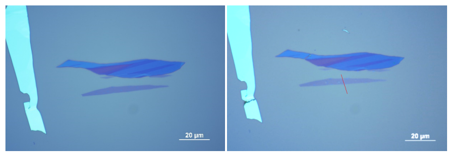
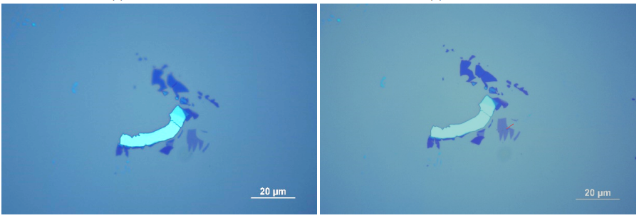
Fig 2.1 - Comparison before and after MoTe2 cutted by AFM
From this, it can be observed that this cutting method is stable and the incision is extremely small.
Transfer Techniques
In order to realize the stacking of 2D materials, the stacking of stacked structures can be realized by various transfer methods. This section will summarize the existing transfer methods and explain the main reasons for choosing dry transfer. Then, this section will detail the dry transfer process and show the twisted samples prepared in this project.
Trasfer Techniques and their comparison
To achieve the stacking of 2D materials, researchers need to transfer the samples. At present, there are the following transfer methods: dry transfer, wet transfer, heat release tape transfer, vacuum hot pressing transfer, bubbling transfer.
The dry transfer method utilizes physical adsorption. It is based on the principle that the interaction force between the polymer and the 2D material is greater than that between the 2D material and the substrate. This method can achieve accurate stacking of samples and transfer without contamination to the surface of the samples, which is the requirement of this project for the higher surface cleanness of 2D materials and the accuracy of sample stacking.
In addition to dry transfer, wet transfer, thermal release tape transfer and other methods are also commonly used. Wet transfer utilizes methods that can directly corrode the substrate or polymer solution-assisted transfer to achieve low-cost, large-area transfer. However, this method was not suitable for this project due to its tendency to wrinkle and the cracked polymer to be difficult to remove. The heat-release tape transfer method takes advantage of the strong adsorption force between the metal film and the 2D material, and uses the heat-release tape to quickly pick up the 2D sample. Although the impurities in the transfer process of thermal release tape are far less than those of wet transfer, it is not the best choice for this project due to the complicated operation process. The thermal release tape can also be used in vacuum hot pressing, layer-by-layer stacking can be realized in a vacuum system, and a large-area multi-layer heterojunction can be prepared. However, due to the introduction of too many difficult-to-remove polymers on the surface of the 2D material, this method is not suitable for this project, which also requires high surface cleanliness.
In addition, some researchers use electrochemical or ultrasonic to generate bubble collapse force to separate the material from the substrate. The device is simple, but it is easy to fold or even rupture. It is also not the best option for this project, either. [25]
To sum up, this project adopts the stacking of twisted structures by dry transfer which can achieve precise transfer and less contamination on the sample surface. Among them, dry transfer is classified according to the transfer tool, and there are three main methods: Polydimethylsiloxane (PDMS), Polycarbonate (PC) and Polypropylene carbonate (Poly Propylene Carbonate, PPC) and PDMS assembly. Since the MoTe2 sample is very easy to oxidize, the oxidized sample cannot be separated from the substrate by ordinary transfer methods. Therefore, in order to improve the success rate of the transfer, the high temperature needs to be raised in a short time during the transfer process. This requires the stability of the film used in the transfer process, so this project uses PDMS and PC with the highest stability as the pick-up tool for transfer.
Dry Transfer Process
In the dry transfer process, we need to prepare a pick-up tool for the transfer process. The pick-up tool is mainly composed of PDMS dicing, PC film, double-sided tape, and glass slide. The preparation process is as follows:
- Cut a PDMS cubic and place it on the slide;
- Place the PDMS block in it with double-sided tape with holes of the same size as the PDMS;
- Use a blue tape with a hole slightly larger than the size of PDMS to stick the PC film;
- Align the holes of the single-sided tape with the holes on the double-sided tape as much as possible, so that the PC and PDMS are closely attached;
- Verify the quality of the pick-up tool by heating at 120℃ for a few seconds;
- Observe if there is comtamination under a microscope;
A high-quality pick-up tool is produced in this way, and a robust transfer can be achieved. Figure 2-2 shows a cross-sectional view of the pick tool.

Fig 2.2 - Pick up tool cross-sectional view
After the pick-up tool is prepared, the sample is transferred using the pick-up tool and transfer equipment. The process is as follows:
- Use the optical photos of the sample to design the twisted structure
- Find the sample under the microscope, compare the design, and use the pick-up tool to pick up and place by heating and cooling many times;
- After stacking the samples, use high temperature to melt the PC film and separate it from PDMS.
- Wash the PC membrane with chloroform to complete the whole transfer process.
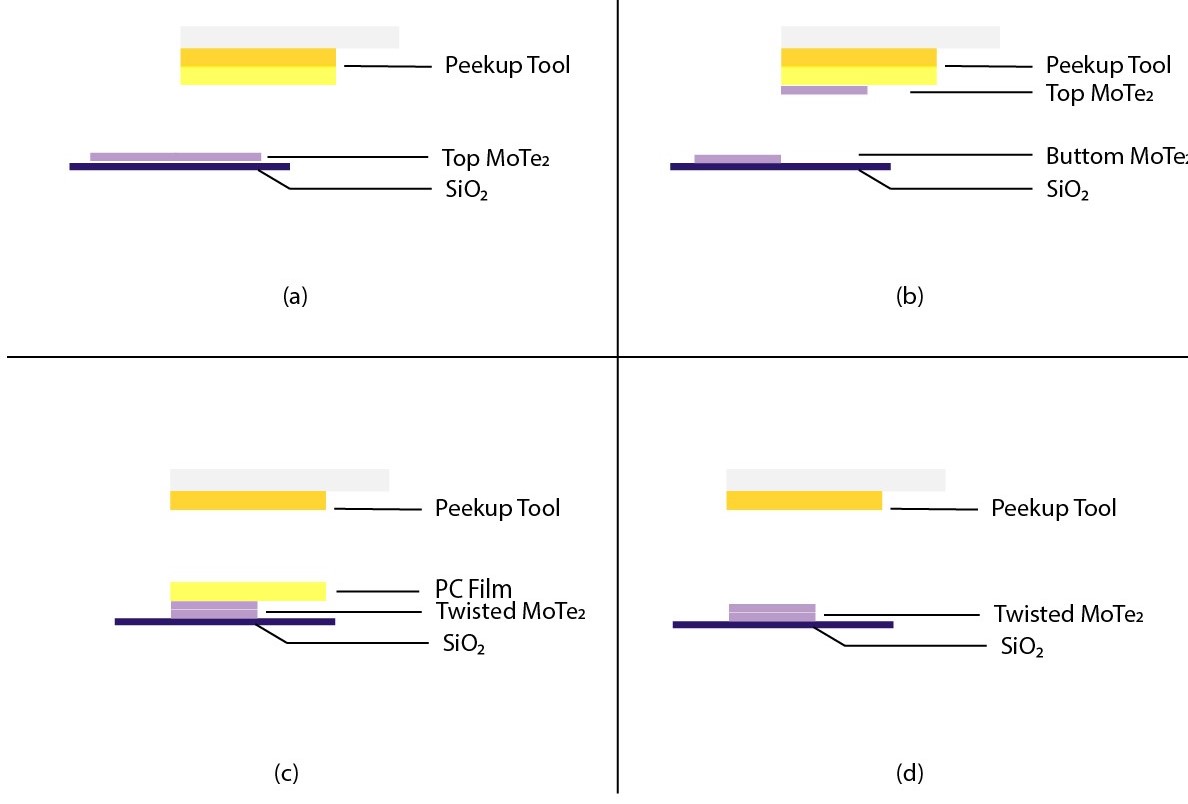
Fig 2.3 - Transfer Process
According to the design requirements, repeat steps three and four to complete the stacking of the 2D structure. The fabrication process is shown in Fig 2.3. Figure (a) shows the pick-up tool ready to pick up the upper MoTe2 layer. Figure (b) shows the pick-up tool successfully picking up the upper MoTe2 sample, adjusting the position according to the design, and preparing to pick up the lower MoTe2 sample. Figure (c) shows that the upper and lower layers of MoTe2 are in contact, and the twisted MoTe2 sample is successfully prepared. Figure (d) shows the final step: the PC film is separated from the pick-up tool, leaving the sample on the substrate.
It is worth noting that since MoTe2 is easily sampled, it is sensitive to temperature, and it is necessary to always pay attention to whether it is oxidized during the transfer process. If oxidized, MoTe2 interacts strongly with the silica substrate, making sample transfer impossible by this method.
Twisted MoTe2 Samples
The following figure shows some twisted qualayer MoTe2 Samples with 29° and 45°. taken under microscope. Red is the overlapping part of the twisted area, and yellow is the non-overlapping part. Compared with the design drawings, these samples can basically be prepared for twisted samples according to the original design. These twisted samples can be as small as 5 microns per side.
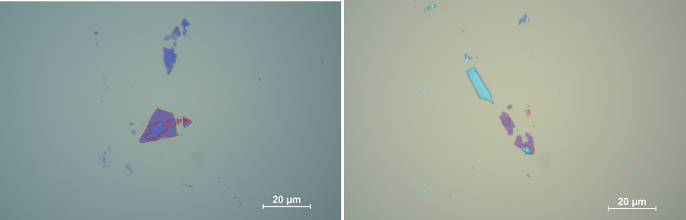
Fig 2.4 - Pick up tool cross-sectional view
Chapter 3: Ramam Spectroscopy Charaterization and Analysis
This chapter mainly focuses on Raman spectroscopy. In the first section of this chapter, the development and basic principles of Raman spectroscopy will be explained in detail, and redefine some of the concepts used in this paper based on these basic knowledge. The second section will give a detailed description of the Raman spectroscopy conditions and test results of the twisted structure of this project. In the third section of this chapter, the Raman test results of the twisted samples are analyzed and the conclusions are obtained. Finally, before the end of this chapter, this paper will organize and summarize the experiments of Raman spectroscopy.
Raman effect and Raman spectroscopy
In 1928, Indian physicist Chandrasekara Raman discovered that the frequency of light waves changed after being scattered again, that is, photons undergo inelastic scattering, which was later named the Raman effect or Raman Scattering. There are two main types of Raman scattering - Stokes scattering and non-Stokes scattering. After the photon transitions from the ground state to the virtual state, the molecule emits a photon to the new energy level because this state is unstable. If the molecule returns to a higher energy level, the emitted photon has less energy, that is, has a longer wavelength than the incident photon, and the vibrational energy of the molecule increases, which is called Stokes Raman scattering. If the molecule returns to a lower energy level, the emitted photon has a larger energy, that is, a shorter wavelength than the incident photon, and the vibrational energy of the molecule decreases, which is called non-Stokes Raman scattering. And if the molecule can return to its original vibrational energy level, then the photon it emits has the same energy as the incident photon, that is, the same wavelength. At this point, no energy is transferred to the molecule, which is Rayleigh scattering. This project mainly explores Stokes scattering.
The function graph of Raman scattering intensity versus wavelength becomes a Raman spectrum, and the abscissa is the wave number (Raman frequency shift) relative to the wavelength of the excitation light, and the wave number is the reciprocal of the wavelength. The Raman shift in wavenumber is calculated as follows:
$Raman Shift(cm^{-1})=\frac{1}{excited \ wavelength nm (\frac{1.0 cm}{10^7 cm})}-\frac{1}{scatter \ wavelength nm (\frac{1.0 cm}{10^7 cm})}$
The Stokes Raman intensity is proportional to the number of molecules in the lowest energy state, while the anti-Stokes Raman intensity is proportional to the number of molecules in the next highest vibrational energy level. According to $\frac{N_1}{N_0}=\frac{g_1}{g_0}exp[-(\Delta E)/KT]$, in the state of thermal equilibrium, the number of molecules in the low vibrational mode energy level is always greater than the number of molecules in the next highest vibrational energy level, so the Stokes Raman intensity is always greater than the anti-Stokes Raman intensity, and its intensity is relatively satisfactory the following formula:
$\frac{I_{Stokes}}{I_{Anti-Strokes}}=\frac{(\vec{v}_o-\vec{v}_M)^4}{(\vec{v}_o+\vec{v}_M)^4}exp(\frac{hc\vec{v}_o}{k_BT})$
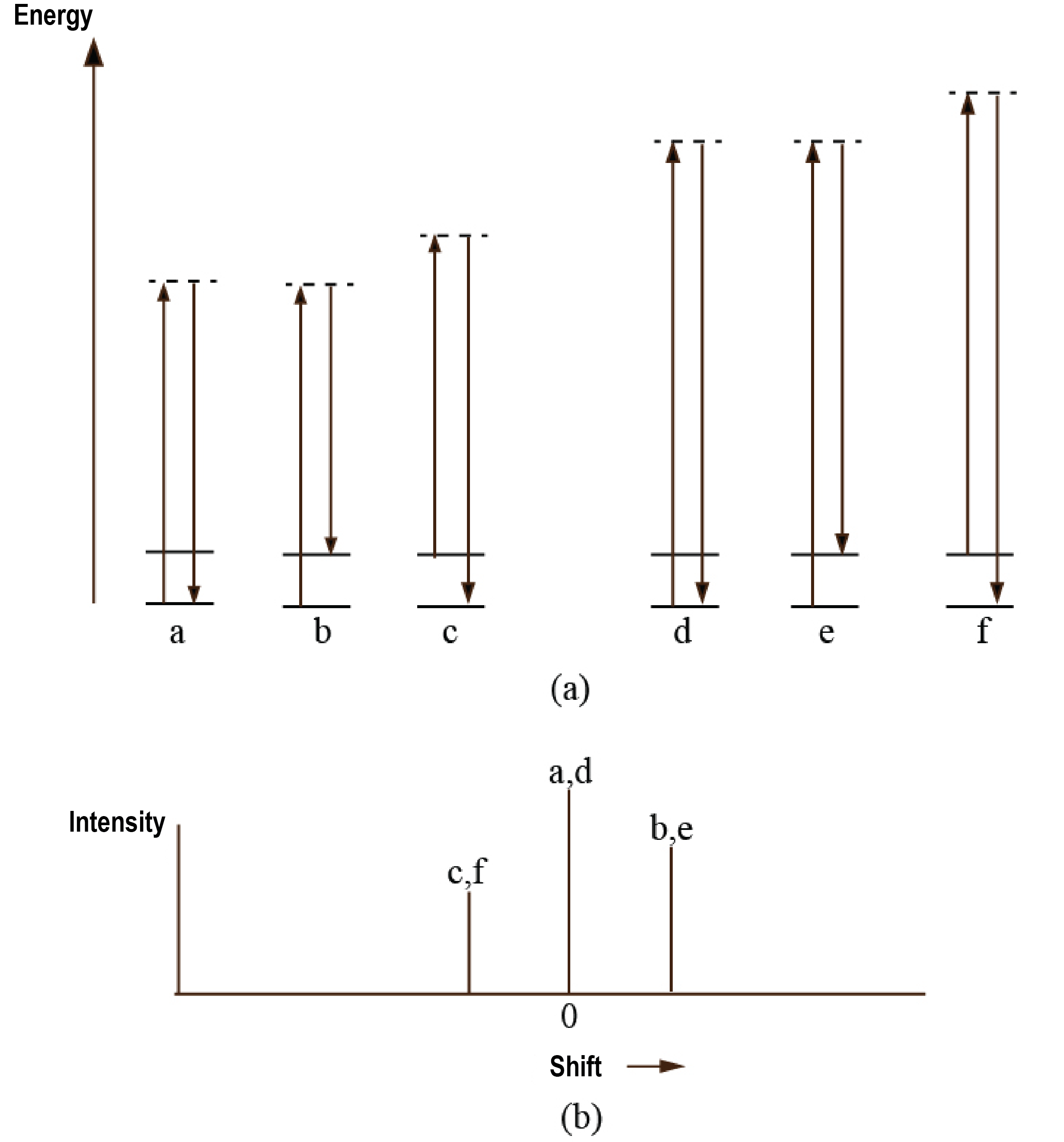
Fig 3.1 - (a) shows the schematic diagram of the energy level transition of Rayleigh scattering, Stokes scattering, and anti-Stokes scattering (b) is the comparison diagram of the frequency shift and intensity corresponding to the scattering case
Figure 3-1 shows the schematic diagram of different scattering energy level transitions in the material and the corresponding frequency shift and intensity comparison diagram. The main research in this project is Stokes Raman scattering. It is worth noting that the wavenumber has the following relationship with the excited energy: $E=hv=\frac{hc}{\lambda}=hc\omega$ , that is, the Raman frequency shift is a measure of the vibrational energy, and the Raman frequency shift can reflect different vibrational energies (quantized vibrations energy levels) to distinguish different vibrational modes (discontinuities exhibited by Raman scattering spectra). [26]
With Raman spectroscopy, we can further characterize material properties. In this project, by understanding the Raman spectrum of the twisted structure, the changes of the vibrational modes displayed by the spectrum is paid attention to for understanding the changes in the atomic arrangement caused by the twisted structure. By characterizing the vibration mode changes caused by the rotation angle, the Raman spectrum changes corresponding to different angles can be inferred, and a deeper understanding of the material can be obtained.
Raman spectroscopy of twisted 2D structures
To characterize the twisted structure of 2D structures, Raman spectroscopy is a commonly used means. Since the twisted structure destroys the original symmetry of the material, the resulting phonon vibrations associated with the interlayer vibrational modes will produce new changes. The change is mainly manifested in the peak position, FWHM and the ratio between different peaks of the twisted structure. By comparing the Raman spectra of the two-layer MoTe2 sample and the four-layer MoTe2 sample, we can understand the changes of the Raman spectra of the twisted structure. Combined with the correlation between Raman spectra and phonon vibrational modes, we can understand the influence of different rotation angles on the interlayer interaction force, and form a one-to-one correspondence between Raman spectra and rotation angles, which becomes the "fingerprint" of twisted MoTe2.
Based on all conditions, this project uses green light with a wavelength of 633 nm to measure the sample. During the measurement, because MoTe2 is sensitive, too high power can cause damage to the sample and oxidize the sample. In order to avoid it, combined with the measurement power mentioned in the literature, the measurement power used in this project is 0.1 mW, and the total time of a single integration is 30 seconds.The measurement data is shown in Fig 3.2.
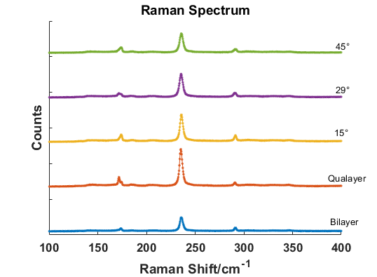
Fig 3.2 - Raman spectra of double-layer, four-layer, 15◦, 29◦, 45◦ twisted samples at 633nm wavelength lights
A total of nine characteristic peaks were measured, and their peak positions were $~138cm^{-1}$, $~171cm^{-1}$, $~138cm^{-1}$, $~ 205cm^{-1}$, $~235cm^{-1}$, $~291cm^{-1}$, $~306cm^{-1}$, $~329cm^{-1}$, $~345cm^{-1}$, these peak positions are similar to those mentioned in the literature. Among them, the two split peaks of $~171cm^{-1}$ correspond to the $A_{1g}$ vibrational mode, which is the mode generated by the relative motion of the molybdenum and tellurium atoms between the upper and lower layers, as shown in Figure 3-3(a) below. The atomic vibrational model for this vibrational mode is clearly demonstrated in , both in terms of the number of layers and the magnitude of the angle. $~235cm^{-1}$ corresponds to the $E^1_{2g}$ peak, which is the interlayer vibrational mode, shown in Figure 3-3(b) below, which represents the motion of the tellurium and molybdenum atoms in the layer, the number of layers and the angle Less affected. $~291cm^{-1}$ represents the $E^1_{2g}$ peak, which is caused by the relative motion of molybdenum and tellurium atoms in the interlayer. The peak position of this characteristic peak is also related to the number of layers and the size of the angle. For $~306cm^{-1}$ the peaks are characteristic of silicon, non-twisted samples or characteristic peaks associated with MoTe2 material. According to the reviewed literature, the remaining five peaks are vibration peaks corresponding to the double resonance Raman of the twisted MoTe2.
Fig 3.3 - in-plane (a) and out-of-plane (b) optical phonon modes of four-layer MoTe2 [27]
In order to study the vibrational modes between the different peaks in more detail, a local amplification analysis of the Raman spectrum was performed. According to the figure, the situation of the $A_{1g}$ peak can be seen more clearly. Splitting occurs in the fourth layer of $A_{1g}$, while the second layer has a larger half width. The relative peak positions of the twisted bilayer samples show double peaks or "shoulders", which fully indicates that the MoTe2 in the upper and lower layers of the twisted bilayer structure has interlayer interactions, and the twisted structure samples were successfully prepared. At the same time, the $A_{1g}$ peak of the twisted structure is very different from that of the four-layer sample, which indicates that the relative rotation angle of the upper and lower two-layer samples has a great influence on the interaction between the layers.
Observing Figure 3.4., comparing the A_{1g} peaks of the five samples, the second layer is a relatively broad peak at $173.6cm^{-1}$, while the fourth peak is split, and the peak positions are located at $171.7cm^{-1}$ and $174cm^{-1}$, respectively. The wavenumbers of the double peaks differ by about $3cm^{-1}$. The two untreated peaks are basically consistent with the bilayer and trilayer peak positions of about $173cm^{-1}$, $171cm^{-1}$ and $173cm^{-1}$ in the literature. These differences may be caused by the measurement system itself, and this difference is acceptable.
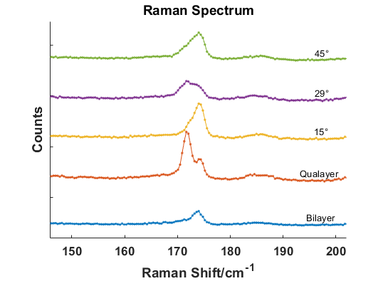
Fig 3.4 - $A_{1g}$ peak of double-layer, qua-layer, 15◦, 29◦, 45◦ twisted samples at 633nm wavelength lights
Comparing the twisted sample with the qua-layer sample and the double-layer sample, it can be found that the spectrum of the twisted sample is more similar to the Raman spectrum of the qua-layer sample, which indicates that the two layers of MoTe2 on the upper and lower layers of the twisted structure have produced interlayer interactions, the qua-layer sample of the twisted was successfully stacked. However, there is a big difference in the splitting of the $A_{1g}$ peak between the spectrum of the twisted sample and the qua-layer sample. For the 15° and 45° samples, since the lattice symmetry period is 30° − θ, the lattice periodicity should be the same at these two angles, and the Raman peak position and full width at half maximum should be similar. Experimental measurements fit this prediction. At the same time, this peak is mainly composed of two peaks. Under different rotation angles, the intensities of different vibration modes are different, resulting in changes in the intensity distribution of Raman peaks. This results in that at different angles, the intensities of the two peaks are similar in some angles, while shoulders are formed in others, and the intensities are quite different. Since 30° − θ will return to the original atomic arrangement, the coupling of the two peaks of the 29° sample will be higher than that of 15° and 45°, and the $A_{1g}$ peak of the 29° sample is observed to couple almost two vibrational peaks into one peak. ,In line with expectations. By comparing the $A_{1g}$ peaks of the three samples, it can be seen that the relative rotation angles of different turning structures can be judged by the $A_{1g}$ peaks at different angles.
At the same time, according to the similar positions and similar shapes of the $A_{1g}$ peaks at 15° and 45°, the following inferences are made: since the atomic arrangement of the rotation angle of 30° − θ and the rotation angle of 30° + θ is the same, the two samples with rotation angles are in the same arrangement. The Raman spectra should be the same. If the Raman spectra of rotation angles from 1° to 59° are compared and plotted, the shift of the peak position of this characteristic peak should form a "v"-shaped curve with 30° as the symmetry axis.
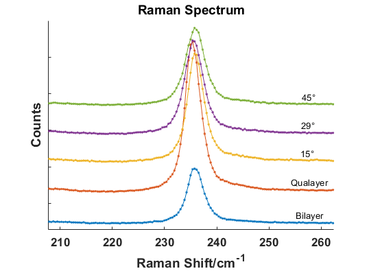
Fig 3.5 - $E^1_{2g}$ peak of double-layer, qua-layer, 15◦, 29◦, 45◦ twisted samples at 633nm wavelength lights
Figure 3.5. shows the $E^1_{2g}$ peaks for the bilayer, qua-layer and twisted samples. Comparing the peaks of $E^1_{2g}$ of the five samples, it represents the relative motion of tellurium atoms and molybdenum atoms in the layer. Figure 3-3(b) can be observed, and the peak position and half-width of the peak remain unchanged. It cannot be a "fingerprint" for judging the size of a twisted degree.
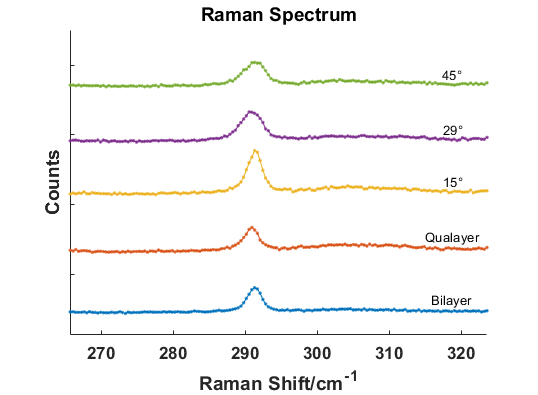
Fig 3.6 - $B^1_{2g}$ peak of double-layer, qua-layer, 15◦, 29◦, 45◦ twisted samples at 633nm wavelength lights
Comparing the $B^1_{2g}$ peaks of the five samples in Figure 3.6., this peak represents the relative movement between the tellurium and molybdenum atomic layers. The number of layers and the rotation angle will affect the peak position and half-width of the vibrational peak. Comparing the qua-layer sample and the twisted sample, it can be found that there is a slight shift in the peak position and in the half-peak width, but the difference is not obvious, which can be used as an auxiliary judgment of the twisted size of the twisted structure. In addition, the peak shift of $B^1_{2g}$, which is closely related to the interlayer interaction, should show a "v"-shaped symmetrical curve similar to that of $A_{1g}$.
The characteristic peak of the double resonance Raman related to the interlayer vibration is only $\omega 4$, but because the peak intensity at this position is not large, and it is more affected by the Raman measurement system, it can only be used as a means to assist the judgment of the size of the rotation angle. It is not the most important best method.
To sum up, for the characterization of the rotation angle of the twisted structure, the best judgment peak is the $A_{1g}$ peak, supplemented by the $B^1_{2g}$ and $\omega 4$ vibration mode peaks. By comparing the difference of the peak positions and half-peak widths of these vibrational peaks, we can understand the changes of the phonon vibrational modes under different rotation angles. This "Raman fingerprint" can be used as one of the verifications for the preparation of the twisted structure in the future.
According to the literature, the appearance of superlattices due to the Moiré pattern should give rise to new vibrational modes due to phonon folding effects. These Moiré Phonon-related vibrational modes have very narrow peak widths at half maximum and often appear near vibrational modes that arise from secondary scattering. However, after careful observation and analysis, this phenomenon could not be observed as expected in this experimental measurement.
Chapter 4: Improvements
As mentioned in the previous chapter, no new vibrational modes associated with Moiré patterns have emerged in the experiments and Raman measurements of this project. There are two main reasons for this phenomenon: the preparation experiment itself and the measurement experiment. In terms of preparation experiments, the interaction between the upper and lower MoTe2 layers is not strong enough to make the superlattice vibration appear in new vibration modes. In terms of measurements, the occurrence of these modes cannot be observed because the vibrational modes caused by secondary scattering may be coupled with the vibrational modes caused by Moiré phonons at specific wavelengths. This chapter will illustrate these two aspects and propose experimental improvement schemes. The tentative experimental results of the current experimental improvement scheme will also be presented in this chapter.
Twisted MoTe2 Fabrication Process
According to the relevant literature, Moiré phonon vibrations are closely related to the interlayer interactions of the twisted structure, which means that the closer the layers are attached, the stronger the interaction, and the more likely it is to observe Moiré phonon-related Vibration mode. In order to improve the interlayer interaction, there are currently three main methods suitable for this experiment: 2D materials surface cleaning, AFM flattening technique, and thermal annealing.
2D Materials Surface Cleaning and Related Work
In order to make the prepared heterostructures have stronger interaction force and closer adhesion between layers, this has higher requirements on the cleanliness of the sample surface. As a result, researchers have developed a variety of surface cleaning methods to treat samples.
One of the most common methods to clean the sample surface with organic solvents is organic solvents. Researchers often use organic solvents such as isopropanol, acetone, and anhydrous ethanol to process samples to dissolve the organics remaining from mechanical cleavage or other growth methods in these strong organic solvents to obtain relatively clean surfaces. However, during the cleaning process, the solvent or part of the organic matter on the sample is evenly distributed on the surface of the sample. The organic matter may float on the surface of the organic solvent, and when the sample is clamped, the organic matter on the surface may be brought back to the surface of the silicon wafer. Although this method is simple, it cannot completely remove the organic matter of the sample, and the residual degree of organic matter molecules is high.
In addition to organic solvents cleaning, thermal annealing is also a common surface cleaning method. Under a certain high temperature, the organic matter on the sample is sublimated and taken away by the airflow under a stable airflow. In order to achieve the cleaning effect, the temperature of thermal annealing needs to be higher. [28]
The researchers also developed an AFM surface cleaning method based on the principle of AFM cutting. The atomic force microneedle uses an appropriate amount of force to continuously scan the surface of the sample, sweeping the raised object to the edge of the sample to achieve a cleaning effect. Without scratching the sample, the greater the force exerted by the atomic force microneedle, the more obvious the cleaning effect. [29]
In addition, in order to adapt to the surface cleaning of 2D materials in different environments, some researchers also use other methods to clean the surface. For example: in a cryogenic oven, it is difficult to anneal the crystal, and the researchers pass an electric current through the sample, and the residual particles are melted into a thin film due to Joule heat, or melted and sublimated to achieve surface cleaning. [31]
The surface cleaning of samples with organic solvents cannot remove all residues from the surface, which cannot meet the requirements of the surface cleanliness of 2D materials in this experiment. For the thermal annealing method, since the high temperature will damage the crystal lattice of the MoTe2 sample, resulting in irreparable damage and affecting the subsequent experimental measurements, it cannot meet the experimental requirements of this project. For the MoTe2 used in this project, which is sensitive to temperature and requires high surface cleanliness, it is a feasible solution to locally clean the surface of the sample through atomic force microscopy. This method can meet the cleanliness requirements of the sample surface for this project, and the sample can be cleaned to a single atomic layer. At the same time, this method does not cause lattice damage to the sample.
Atomic Force Microscope Surface Cleaning
In order to clean the surface of the underlying 2D material, this project attempts to use AFM for surface cleaning. AFM surface cleaning is a localized, fine and almost non-destructive cleaning method. The surface cleaning of 2D materials can be achieved by controlling the appropriate force, that is, the force with which the AFM probe is closely attached to the surface of the sample without being scratched. The following shows the process:
- Replace the AFM probe dedicated to the contact mode;
- Position the sample under the microscope;
- Scan the topography of the sample using the semi-contact mode;
- Set the appropriate contact strength and scanning frequency, and scan the sample with the contact mode, and the scanning range is the area that needs to be cleaned;
- Clean several times until the required area surface is clean;
- Scan the topography of the sample using the semi-contact mode;
In a preparative experimental refinement, an attempt was made to use AFM for surface cleaning, using less force than the force used for cutting. After two cleanings, it was observed that cleaning the surface by AFM contact mode does work. Before cleaning, the thickness of the sample was about 4nm. After cleaning by atomic force microscope, the thickness of the sample is reduced to nearly 1.5nm, which is close to the thickness of one atomic layer. Comparing the two, the difference between the uncleaned area and the cleaned area is 2.39 nm. This fully demonstrates that the scanning in the contact mode of the atomic force microscope has a good cleaning effect on the surface of the sample, and this method of cleaning the surface is feasible.
Fig 4-1 - AFM Surface Cleaning
Figure 4.1. shows the AFM samples before and after cleaning. The area enclosed by the red outline in the right image of Figure 4-1b is the cleaned area. Comparing the cleaned area and the uncleaned area, it can be seen that the particles in the cleaned area are significantly reduced, and the surface is more uniform, which intuitively shows the effect of atomic force microscope surface cleaning.
By cleaning the organic molecule residues in the lower layer sample by this method, the influence of organic molecules between the upper and lower interlayers can be reduced, thereby reducing the distance between the layers, or improving the interaction force between the layers.
Interlayer Interaction Enhancement Techniques
In addition to surface cleaning of the samples before preparation, the interlayer interaction can also be enhanced after preparation of the twisted samples. According to the literature read so far, there are two applicable methods: AFM flattening technique and thermal annealing method.
AFM Flattening
For twisted samples, the relative rotation angle increases the distance between the upper and lower layers. The larger the angle of relative rotation and the larger the distance, the greater the negative impact on the interaction between layers. In this project, AFM can not only be used for cutting and surface cleaning of the underlying sample surface, but also to enhance the interaction between layers through AFM flattening technology.
According to relevant literature, due to the uneven substrate and insufficient pressing force during mechanical cleavage, the thickness of graphene is higher than that of a single layer of atoms, which shows that graphene is not tightly combined with the substrate. A close contact between the graphene and the substrate is achieved through the contact mode scanning of the atomic force microscope - to achieve flattening. Similar turning angle samples are not equal to the thickness of two layers of samples stacked directly, and the interaction is not tightly bound and the distance brought by the relative turning angle affects the interaction. Similar to surface cleaning, this method physically flattens the sample. The enhanced interaction is achieved by applying the appropriate force to the 2D sample, that is, the force that is tightly bound to the sample surface but fails to scrape the sample, scans the sample surface in AFM contact mode and reduces the thickness of the twisted sample force effect. This method does not cause damage to the sample surface and is the appropriate method for this project. The stronger the scan, the more obvious the cleaning effect. [30]
Heat Annealing
According to relevant literature, the method of thermal annealing can remove the organic matter in the layer from the interlayer of the twisted structure under the dual action of high temperature and air flow, realize the cleaning in the layer and enhance the interaction force between the layers. At the same time, some related literature show that some modes cannot be excited due to the large interlayer distance in the unannealed sample. Since Moiré patterns are closely related to interlayer interactions, it is speculated whether annealing is a necessary experimental procedure to observe vibrational peaks associated with Moiré phonons. [32]
When annealing temperature is between 150℃ and 200℃ in hydrogen and argon atmosphere.After the test after the experiment, this condition has no obvious negative effect on the Raman signal of molybdenum telluride, which can be applied to this project. [33,34]
It is worth noting that some documents also mentioned that the high-temperature thermal annealing of the twisted graphene sample would change the angle of rotation and untwist. However, since the temperature has not reached very high, and the rotation angles of the twisted samples prepared in this project are all large, the influence of thermal annealing on the angle is within an acceptable range, so this method can be used to improve the interlayer interaction of the twisted samples. effect.
Twisted MoTe2 Raman Spectroscopy
In this project, 633 nm excitation light was used for Raman spectroscopy measurements. According to Tan's research on MoS2 with constant rotation angle, the peak position and intensity of the vibrational peaks related to Moiré phonons under the excitation of different wavelengths of light will change. These characteristic peaks may be indistinguishable from those of the second-order Raman, so the Raman test from 1.83 eV-2.81 eV was performed. According to the results of this study, when the intensity of the excitation light is close to that of the C excitons of MoS2, the intensity of the modes associated with the Moiré phonon vibrational modes is enhanced, thereby inferring the resonance Raman effect of the moiré phonon is produced by the exciton effect. This means that the choice of excitation light intensity will affect the measurement of the Moiré phonon vibrational mode, so the subsequent experiments need to adjust the wavelength of the measurement to further understand the vibrational modes related to the twisted MoTe2.
In addition to the need to perform Raman measurements of different wavelengths on the twisted samples, in order to fully understand the effect of moiré patterns on phonon vibration, low-wavenumber Raman should also be one of the research topics of twisted MoTe2, which should be further studied in the follow-up research.
Further Research
Further Research is still ongoing now. The project is taken over by Shiyuan Wang.
Conclusions
This project mainly focuses on the study of the phonon vibration mode of twisted MoTe2. Through the process of mechanical cleavage, atomic force microscope cutting, and dry transfer, bi-layer and qua-layer were prepared, and the samples were measured in Raman Spectroscopy under excitation light of 633 nm. By analyzing the Raman spectra, the following conclusions are drawn: the $A_{1g}$ and $B^1_{2g}$ peaks related to the interlayer interaction can be used as the basis for judging the rotation angle of the twisted MoTe2. According to the symmetry of the atomic arrangement, it is predicted that the Raman frequency shift positions of these two vibrational modes of the twisted molybdenum telluride sample will form a "v"-shaped curve with 30° as the axis of symmetry between 1° and 59°. In this project, Raman vibrational modes associated with Moiré phonons were not expected to be observed.
This project speculates that the failure to observe the Raman vibration peaks related to Moiré phonons is mainly due to the insufficient interlayer interaction force of the twisted sample and the wrong choice of wavelength for measurement. Based on the relevant literature and the results of subsequent exploratory experiments, this project proposes the following experimental improvements: AFM surface cleaning, AFM flattening technology, and thermal annealing technology. At the same time, other wavelengths of measurement light and low-wave number Raman measurements were added to complete the study of all phonon modes of twisted MoTe2.
This project develops a stable twisted structure preparation scheme for 2D materials with relatively small areas that can only be obtained by mechanical cleavage methods. Without other 2D as supplement layers, it is friendly to the low-wavenumber Raman research in the follow-up on the interlayer interaction of the twisted 2D materials.
Because Raman research is a powerful characterization method for comprehensively exploring all phonon modes of materials, and phonon vibrational modes can reflect crystal structure, crystal symmetry, defects and impurities, the development of stable twisted preparation technology enables more twisted samples The research is conducive to a clearer and comprehensive understanding of the mechanical properties, thermodynamic properties, electrical properties, optical properties and other material properties of this two-dimensional material system, and provides reference information for future device preparation and selection of material systems. The prepared twisted samples may also be used for the measurement of light absorption, photoluminescence, and second harmonics. The comprehensive characterization of the twisted samples will help to enhance the understanding of the properties of the twisted samples, and to apply their special properties to more in special devices.
In addition, understanding the physical mechanism of phonon regulation of Moiré patterns is also conducive to the further development of "phonon engineering" to provide a physical basis for the preparation of devices with excellent phonon regulation.
Reference
[1] MOORE G E. Cramming More Components onto Integrated Circuits[J]. Scandinavian Journalof Statistics, 1965, 39(3) : 399 - 415.
[2] NOVOSELOV K S, JIANG D, SCHEDIN F, et al. Two-dimensional atomic crystals[J]. Proceedings of the National Academy of Sciences of the United States of America, 2005, 102(30) :10451 - 10453.
[3] GAO X-G, LI X-K, XIN W, et al. Fabrication, optical properties, and applications of twisted two-dimensional materials[J]. Nanophotonics, 2020, 9(7) : 1717 - 1742.
[4] PONG W T, DURKAN C. A review and outlook for an anomaly of scanning tunnelling microscopy (STM): Superlattices on graphite[J]. Journal of Physics D: Applied Physics, 2005, 38(21).
[5] RONG Z Y, KUIPER P. Electronic effects in scanning tunneling microscopy: Moiré pattern on a graphite surface[J]. Physical Review B, 1993, 48(23) : 17427 - 17431.
[6] BISTRITZER R, MACDONALD A H. Moiré bands in twisted double-layer graphene[J]. Proceedings of the National Academy of Sciences of the United States of America, 2011, 108(30) : 12233 - 12237.
[7] PARK J M, CAO Y, WATANABE K, et al. Tunable strongly coupled superconductivity in magicangle twisted trilayer graphene[J]. Nature, 2021, 590(October 2020).
[8] YU H, LIU G B, TANG J, et al. Moiré excitons: From programmable quantum emitter arrays to spin-orbit coupled artificial lattices[J]. SCIENCE ADVANCES, 2017, 3(e1701696) : 1 - 8.
[9] JIN C, KIM J, SUH J, et al. Interlayer electron-phonon coupling in WSe 2/hBN heterostructures[J]. Nature Physics, 2017, 13(2) : 127 - 131.
[10] LIN M L, TAN Q H, WU J B, et al. Moiré phonons in twisted bilayer MoS2[J]. ACS Nano, 2018, 12(8) : 8770 - 8780.
[11] CHEN X D, XIN W, JIANG W S, et al. High-Precision Twist-Controlled Bilayer and Trilayer Graphene[J]. Advanced Materials, 2016, 28(13) : 2563 - 2570.
[12] ALEXEEV E M, RUIZ-TIJERINA D A, DANOVICH M, et al. Resonantly hybridized excitons in moiré superlattices in van der Waals heterostructures[J]. Nature, 2019, 567(7746) : 81 - 86.
[13] CAMPOS-DELGADO J, CANÇADO L G, ACHETE C A, et al. Raman scattering study of the phonon dispersion in twisted bilayer graphene[J]. Nano Research, 2013, 6(4) : 269 - 274.
[14] FERRARI A C, MEYER J C, SCARDACI V, et al. Raman spectrum of graphene and graphene layers[J]. Physical Review Letters, 2006, 97(18) : 1 - 4.
[15] KIM K, COH S, TAN L Z, et al. Raman spectroscopy study of rotated double-layer graphene: Misorientation-angle dependence of electronic structure[J]. Physical Review Letters, 2012, 108(24) : 1 - 6.
[16] JORIO A, CANÇADO L G. Raman spectroscopy of twisted bilayer graphene[J]. Solid State Communications, 2013, 175-176 : 3 - 12.
[17] HA S, PARK N H, KIM H, et al. Enhanced third-harmonic generation by manipulating the twist angle of bilayer graphene[J]. Light: Science and Applications, 2021, 10(1).
[18] QUAN J, LINHART L, LIN M L, et al. Phonon renormalization in reconstructed MoS2 moiré superlattices[J]. Nature Materials, 2021.
[19] LIN K Q, HOLLER J, BAUER J M, et al. Large-scale mapping of moiré superlattices by Raman imaging of interlayer breathing mode and moiré phonons[J]. arXiv, 2020 : 1 - 20.
[20] NICOLOSI V, CHHOWALLA M, KANATZIDIS M G, et al. Liquid exfoliation of layered materials[J]. Science, 2013, 340(6139) : 72 - 75.
[21] JOENSEN P, FRINDT R F, MORRISON S R. Single-layer MoS2[J]. Materials Research Bulletin, 1986, 21(4) : 457 - 461.
[22] CAO Y, LUO J Y, FATEMI V, et al. Superlattice-Induced Insulating States and Valley-Protected Orbits in Twisted Bilayer Graphene[J]. Physical Review Letters, 2016, 117(11) : 1 - 5.
[23] ZHOU Y, BAO Q, VARGHESE B, et al. Microstructuring of graphene oxide nanosheets using direct laser writing[J]. Advanced Materials, 2010, 22(1) : 67 - 71.
[24] PUDDY R K, SCARD P H, TYNDALL D, et al. Atomic force microscope nanolithography of graphene: Cuts, pseudocuts, and tip current measurements[J]. Applied Physics Letters, 2011, 98(13) : 2 - 4.
[25] KIM C, YOON M-A, JANG B, et al. Review on Transfer Process of Two-dimensional Materials[J]. Tribology and Lubricants, 2020, 36(1) : 1 - 10.
[26] 杨序钢, 吴琪琳. 拉曼光谱的分析与应用 [M]. 北京 : 国防工业出版社, 2008.
[27] Guillaume Froehlicher,† Etienne Lorchat,† François Fernique,† Chaitanya Joshi, Alejandro Molina-Sánchez,‡ Ludger Wirtz , BERCIAUD* S. Unified Description of the Optical Phonon Modes in N‑Layer MoTe2[J], 2015
[28] CHENG Z, ZHOU Q, WANG C, et al. Toward intrinsic graphene surfaces: A systematic study on thermal annealing and wet-chemical treatment of SiO2-supported graphene devices[J]. Nano Letters, 2011, 11(2) : 767 - 771.
[29] LINDVALL N, KALABUKHOV A, YURGENS A. Cleaning graphene using atomic force microscope[J]. Journal of Applied Physics, 2012, 111(6).
[30] ROSENBERGER M R, CHUANG H J, MCCREARY K M, et al. Nano-”Squeegee” for the Creation of Clean 2D Material Interfaces[J]. ACS Applied Materials and Interfaces, 2018, 10(12) : 10379 - 10387.
[31] MOSER J, BARREIRO A, BACHTOLD A. Current-induced cleaning of graphene[J]. Applied Physics Letters, 2007, 91(16) : 1 - 4.
[32] PURETZKY A A, LIANG L, LI X, et al. Twisted MoSe2 Bilayers with Variable Local Stacking and Interlayer Coupling Revealed by Low-Frequency Raman Spectroscopy[J]. ACS Nano, 2016, 10(2) : 2736 - 2744.
[33] ZHENG X, WEI Y, DENG C, et al. Controlled Layer-by-Layer Oxidation of MoTe2 via O3 Exposure[J]. ACS Applied Materials and Interfaces, 2018, 10(36) : 30045 - 30050.
[34] ZHU H, WANG Q, CHENG L, et al. Defects and Surface Structural Stability of MoTe2 under Vacuum Annealing[J]. ACS Nano, 2017, 11(11) : 11005 - 11014.