
EECS425 Coursework Project
Duration: 02/2022-05/2022
Teammates: Daniel Garan, Zhenzhen Gu, Meng-Lin Hseih, Yan Yang
Unfinished Typography
Introduction
Precise positioning of mechanical components is important for many applications. These positioning components can be used as micro-mirrors or lenses in optical application [1,2,3] or they could serve as actuators in scanning probe microscopy [4,5] , sensors in micro-force measuring [6,7] , or even used in data storage systems [8,9,10] . According to the applications, these mechanical positioning components may require different operation specifications, for example limitations in component sizes, requirement for specific natural frequencies, or the need for a certain maximum displacement. To fulfill these different kinds of specification goals, the use of microelectromechanical systems (MEMS) technology has been investigated intensively. MEMS technology is desirable in designing and fabricating these micro/nano positioning components due to its advantages of small sizes and its numerous available sensing/actuating schemes to meet the required specs for different applications.
For the use of nano stages in metrology applications, several different types of MEMS positioning stages have been investigated including electrostatic, thermal and piezoelectric actuated positioning stages. [11,12,13] However, based on the fabrication techniques in this course, Thermal actuation methods were the most suitable design. It is because these actuating methods do not require the use of exotic materials or electrical isolation, making it compatible with general IC fabrication. Another outstanding feature for thermal actuating is that various kinds of displacement amplification schemes are available.
Traditional sensors made of metal foils and semiconductor piezoresistive elements have limited sensitivity, high temperature dependence and are not compatible with standard CMOS integration, making them unsuitable for high-performance and low-cost applications. However, MEMS capacitive sensors have key advantages such as high sensitivity, minimal temperature dependance, low noise, large dynamic range and potential monolithic integration with low-power MOS electronics. Our design is aimed at a high-sensitivity low-noise Nano-stage.
Microsystem Operation
In this design, the capacitive MEMS sensor is integrated with a low-noise CMOS circuit. The CMOS circuit(Capacitive Sensing Amplifier, Mixer, Low Pass Filter, Digital Analog Converter and Controller) utilizes a closed-loop architecture by sensing capacitance change from the stage and controlling its movement by driving circuit based on users' instructions. Signal from the driving circuit will actuate the MEMS stage, leading it to the right place. Meanwhile, the sensing part from the circuit will give real time feedback to the controller in order to adjust the provided actuating voltage. The real time feedback can also translate into displacement. AC signal will be provided for sensing circuit and DC signal will be the actuation supply. This research takes advantage of the displacement amplifying scheme available for thermal actuators to maximize displacement and incorporates a mirrored mechanical design to avoid rotation. Furthermore, a closed loop circuit then further enhances the precision of the translation nano stage. Fig 1. shows General block diagram of the whole micro-system.

Fig 1. - Block Diagram of Microsystem
| Specs | Target |
|---|---|
| MEMS | |
| Mximum Displacement($\mu$ m) | 10 |
| Mximum $\Delta C$(fF) | 20 |
| $C_0$(fF) | 400 |
| Circuit | |
| Mximum $\Delta C$(fF) | ~0.5 |
| Feedback Capacitance | 50fF-2pF |
| Bandwidth(CSA)(MHz) | 4 |
| Output Swing(mV) | 100 |
| Open loop gain CSA(dB) | 90 |
| Closed loop gain CS(dB) | -30 |
MEMS Design
In this session, the design and simulation results will be detailed disscussed.
Design
As shown in Fig.2, the thermally-actuated MEMS translation stage consists of a center released silicon stage, force transmitting and displacement amplifying arms, electrical ports(actuation post, sensing port and ground port) and bottom electrodes. The actuation ports serve as the displacement actuators.
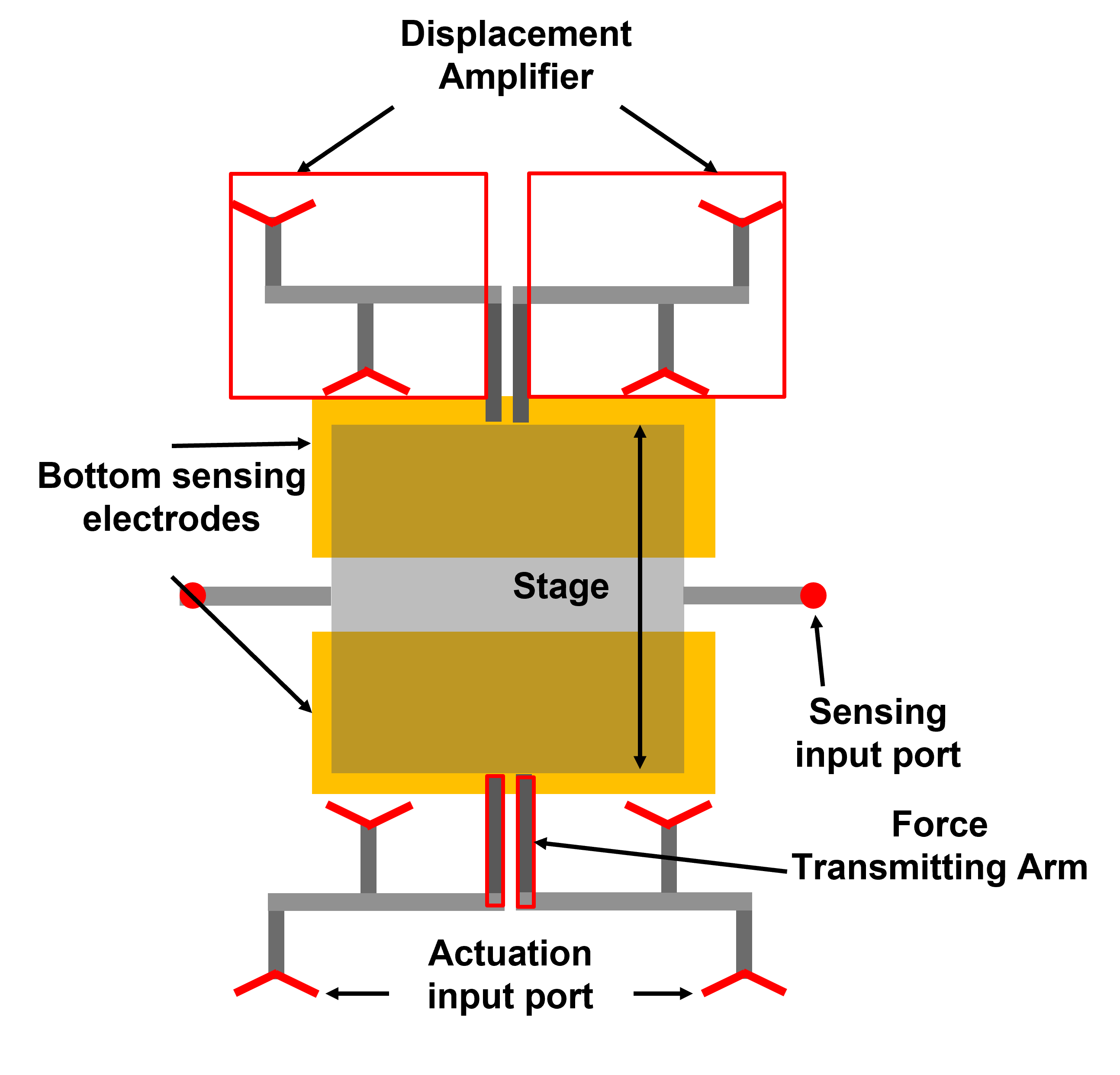
Fig 2. - Top view of the MEMS positioning stage, including center silicon stage, force transmitting and displacement amplifying arm, electrical ports and bottom electrode.
The working principle of the MEMS device is that an input current(I) is applied at the actuation port on the thermal actuators.The Joule heating caused by the current will create a temperature change.($\Delta T$) This will lead to a displacement(disp) due to the thermal expansion of the the actuators. The displacement amplifying arms that are connected to the thermal actuators are used to amplify the thermal displacement and will transmit the amplified displacement(disp*) on the center stage through the force transmitting arms. In the end, the position changes of the center stage due to the thermal actuation will lead to a change in the overlap area between the center stage and bottom sensing electrodes. With the center stage serving as one part of the parallel plate capacitor, and the bottom sensing electrodes serving as the other part, the change in capacitance can be sensed. The whole process will be shown in Fig. 3.
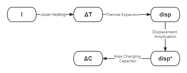
Fig 3. - Working principles of MEMS stage.
The design is also limited by the area(Electrode Pad), which is required to be $2mm \times 2mm$. Additionally, to avoid temperature jump to extremely high locally, the input current should be less than 0.25A. However, based on the primary stimulation results, at least 0.2A on a single port could make the stage move when the stage could move in 2 DOF. In order to have the maximum displacement, 1 DOF is sacrificed. And one chevron requires four driving pads (two actuation pads, two group pads).
When moving in 1 DOF, potential rotation is taken into consideration. The thermal actuators and the displacement amplifying arms ,as well as the force transmitting arm, are mirrored design. This mirrored structure is extremely important to limit the movement in Y-direction and avoid rotation in X-direction.
The optimization of the dimensions for the MEMS devices(the width and length of chevrons, the width and length of arms, the distance between to supporting beams and so on) was verified through COMSOL simulation.
Thermal analysis was conducted in COMSOL to ensure that thermal actuators were operating at a tolerable temperature. Naturally, the higher temperature the actuators are, the more thermal expansion and thus displacement the device will be able to achieve. Based on the maximum operating temperature of around 1000K for a similarly designed thermal actuator in paper, we aimed to design the stage maximum operating temperature of 1000K. Fig 4 shows the temperature simulation results of the actuator and the stage. The square and circle-labeled lines show the simulation results with a temperature-correct conductivity for silicon. Based on these results, nonlinear increase in temperature with respect to an increase in input current. The maximum temperature can be reached within the current limit in this design.
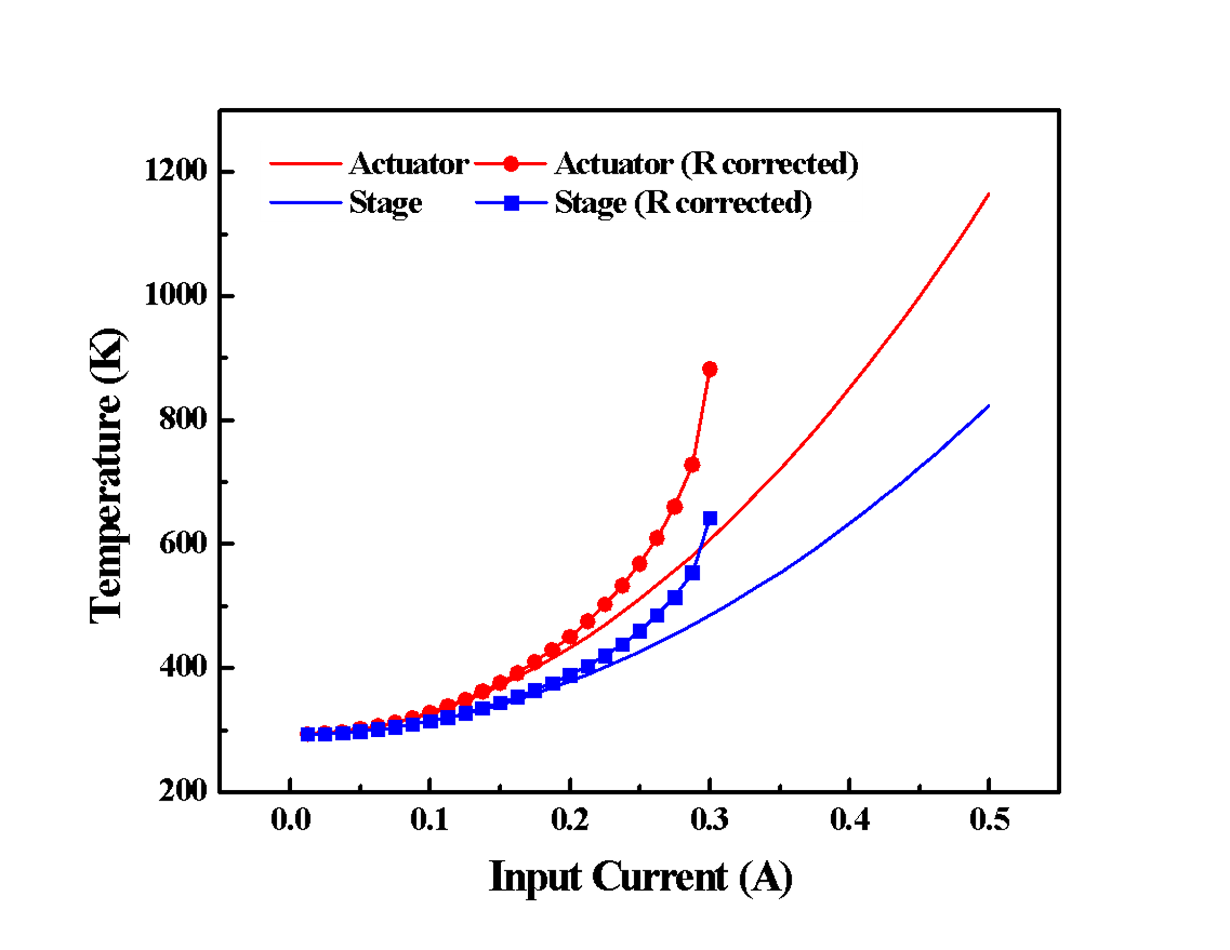
Fig 4. - Temperature analysis of stage
Electrical analysis was also conducted to ensure the potential drift at the center stage was under acceptable level. There are two main causes leading to the electrical potential value of the stage during actuation: (1) MEMS structure is not electrically isolated different components (The structure is not only mechanically, but also electrically connected) (2) Stage is one part of the sensing electrode and play a important role in sensing circuit. A large potential drift during actuation may drive the circuit bias out of working range. The simulation results in Fig 5 shows that the stage potential is affected by input current. However, the potential can be kept under 1.8V of the interface circuit within the driving range of 0.5A.(Two pads drive one chevron.)
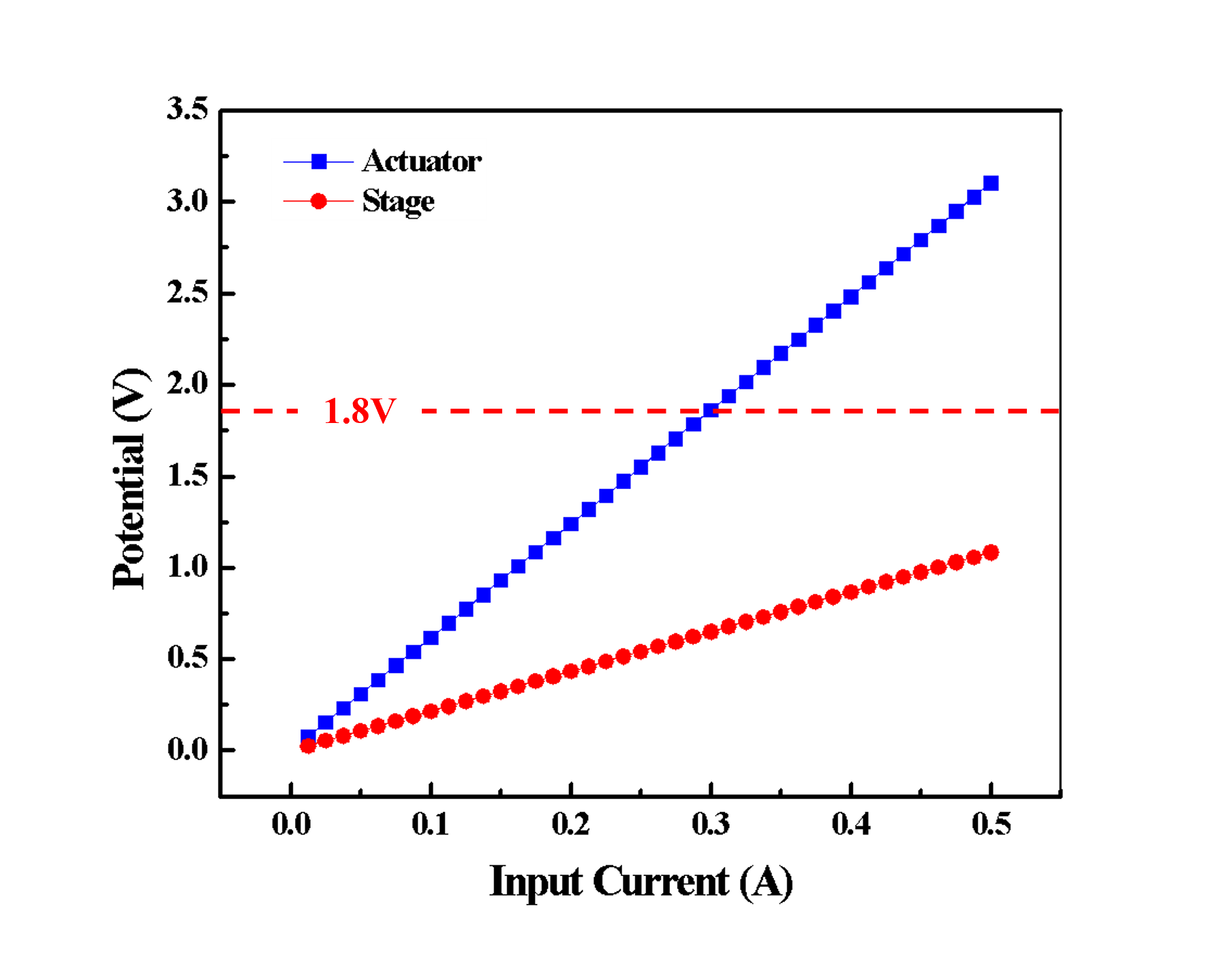
Fig 5. - Electrical analysis of stage
Next, two mechanical analyses were conducted to verify the performance of the MEMS structure. Rotation analysis is to ensure the stage undergoes pure translational motion, while actuation analysis is to calculate the maximum displacement achievable. The results are shown in Fig 5 respectively. The simulation results show that displacement amplifying arms were effective and an amplification factor of around 5.7 was achieved. The center stage was able to achieve $13 \mu m$ of displacement when the actuators are at the maximum operating temperature of 1000K.
In the end, the overall expected capacitance output of the area-changing sensing capacitor was calculated from the simulated displacement results. Fig 6. shows that the sensing capacitor of each is able to reach a maximum capacitance change($\Delta C$) of 19.1 fF atan initial capacitance($C_0$) of 350fF.
Fabrication Process
The process begins with a silicon wafer with a bare $500\mu m$ thick glass wafer. After evaporation of 1000Å Cr as glass etch mask, photoresist is then spined on the metal layer and exposed with GLASS RECESS mask. The Cr without photoresist protection is then etched and stopped until the glass recess reaches the depth of $3\mu m$. Cr and photoresist are striped at this time.
In the second mask process, the bottom electrode is deposited and patterned at this time50Å Cr and 500Å Pt will be deposited respectively after bottom electrode opening is patterned. After Lifting off the Cr/Pt and photoresist, the bottom electrode layer is left behind.
In the third mask process, the whole wafer is bonded $100\mu m$ Silicon and deposited 5000ÅAl. Photoresist is also the protection layer. In the end of this step, the contact metal layer is successfully patterned on the wafer.
In the last step, photoresist works as the protection layer for Si wafer in the DRIE process. Finally, the photoresist is removed and the MEMS stage.
Fig 6. - Fabrication process
Circuit Design
In this session, design and simulation results for custromized circuits willbe discussed in detail.
The following table shows the specs of each components.
| Specs | Target | Result |
|---|---|---|
| CSA | ||
| Open-loop gain | 90 dB | 87.85 dB |
| Close-loop gain | -30 dB | -29.63 dB |
| Bandwidth | 4 MHz | 3.4 MHz |
| Phase margin | 90 deg | 85.5 deg |
| $\beta$ | 0.08 | 0.071 |
| $f_T$ | 50 MHz | 47 MHz |
| $f_L$ | 50 MHz | 47 MHz |
| $f_H$ | 4 MHz | 3.38 MHz |
| Mixer and LPF | ||
| Gain | 10 dB | 9.8 dB |
| Mixer f_{3dB} | 10 dB | 13 dB |
| LPF f_{3dB} | 1.5 kHz | 1.5 kHz |
Capacitive Sensing Amplifier(CSA)
To amplify the signal from the MEMS stage, capacitive sensing amplifier(CSA) is designed for the stage. CSA is a two-stage Miller op-amp with PMOS input pairs. By using this architecture, By connecting $C_f$ as feedback capacitor, the gain, bandwidth and other parameters can be trade off better.
There are two CSA in the circuit. The inputs (negative and positive) of one CSA are the interface ports from the MEMS. The other CSA inputs are dummy capacitors for comparison.
Fig 7. and Fig 8. is the simulation results of Open-looped CSA and Close-looped CSA.
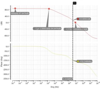
Fig 7. - Open-loop CSA simulation results(AC Analysis)
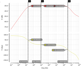
Fig 8. - Close-loop CSA simulation results(AC Analysis)
Mixer and Low Pass Filter(LPF)
Mixer compares two outputs from the CSA and compares the capacitor change. Mixer consists of a fully differential op-amplifier, demodulator and common-mode feedback. Demodulator is implemented with 4 NMOS switches. Miller compensation is implemented for common-mode feedback(CMFB). [14]
Parameters of op-amp in CSA and mixer are completely the same. As for the CMFB, the transistors are fine-tuning based on the gain and frequency.
The output waveform shows in Fig. 9. is the AC simulation of the mixer. By comparing two inputs, the output is the results from the capacitance change. From the simulation results, Linearity and enough amplification could be told.
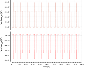
Fig 9. - Mixer simulation results(AC Analysis)
After filtering noise, Fig 10. shows overall simulation result sweep with different $\Delta C$. The linearity decreases as $\Delta C$ approaches 20fF but the overall linearity is workable with a sensitivity of 3.5mV/fF.
Fig 10. - Output signal with different $\Delta C$
Digital Analog Convertor(DAC)
The DAC uses an R2R ladder due to its simplicity and ease of implementation. This consideration also provides a clean signal with low power consumption. Fig 11. shows the simulation results for the R2R ladder. The DAC can supply 256 evenly spaced voltage levels, corresponding to 256 discrete stage positions.
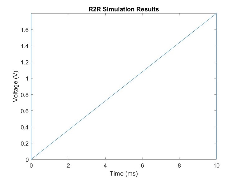
Fig 11. - Simulation results for the DAC.
Controller
The controller compares the user's desired stage(the output of the DAC) and the sensed stage position(the output of the sensing circuit). After that, the actuating signal will change until the difference between the two inputs is zero. According to the simulation results, the design results in a slightly underdamped response with correct output and a very quick response time of 7.14ns.
Noise and Power Consumption Analysis
Noise will affect the overall performance of the customized circuit. Noise is an unwanted signal that creates disturbance to the desired signal content in the system. This can be an additional signal that is produced by the system or can be some disturbance accompanied with the desired information of the input signal. CSA is the main source of noise for the signal chain. Therefore, it is necessary to have LNF followed before.
And power consumption is also important to the circuit, which is expected to be low. It is calculated from the circuit current of the operational amplifier itself and from the output load current.
The following table shows the noise and power consumption of CSA and Mixer. The power and noise from LPF can be neglected.
| Componentsm | Noise | Power |
|---|---|---|
| CSA | 360 $\mu$Vrms | 208.7 $\mu$W |
| Mixer | 125 $\mu$Vrms | 176.4 $\mu$W |
Test
In this session, the testing process and results will be presented. The overview graph in the microscope of the MEMS devices during testing has been shown in Fig 12. Two types of vernier scales were utilized to characterize the motion of displacement of the center stage. Combining information from two vernier scales together regarding the X,Y displacement, the rotational motion can also be known during actuation. The horizontal vernier scale indicates that the mirrored structural design was effective in minimizing any rotational motion occurring rendering the displacement of the center stage almost purely translational.
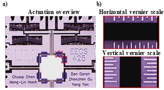
Fig 11. - a) Micrograph overview of the fabricated MEMS devices, and b) zoom-in micrographs of the horizontal and vertical vernier scales used for measuring stage displacement.
Before measuring the stage overall displacement, resistance of two different types of chevrons measures first in order to be compared with theoretical simulation. The two different types of chevrons differ in pairs of actuating legs, and thus should in theory show different values in electrical resistance, $R_{small}$ and $R_{large}$. Fig 12 b). shows the simulation and measurement results of resistance of a single chevron. The simulated results and the measured results also indicate an increase in resistance as input current increases, reflecting the effect of increased phonon scattering that decreases the carrier structure and thus conductivity of the heavily doped silicon structure. However, different from the ideal simulated resistance, the measured results do not show a large difference in resistance between $R_{small}$ and $R_{large}$. It might be because single measured results are outlying data points. It might also be because there is no electrical isolation between chevrons. More thorough experimentation is needed to produce more accurate quantitative results of the chevron resistances.
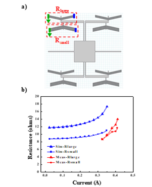
Fig 12 a) Schematic of two types of chevron design, respectively with resistance $R_{large}$ and $R_{small}$ and, b) measurement and simulation results of resistances of a single chevrons for $R_{large}$ and $R_{small}$
Furthermore, in Fig 13. shows the displacement of the center stage changes as the currents increase. As the input current changes from 0.3A to 0.4A, the center stage deforms by 3.33 $\mu m$ to 22.2 $\mu m$ with the breakage occurring at 0.39 A with displacement of 13.9 $\mu m$. Due to the lower measured resistance of the chevron, compared to the simulated resistances, a larger input current is required to displace the center stage. This results in a right shifted measured displacement curve in red compared to the R-corrected simulation displacement curve in blue.
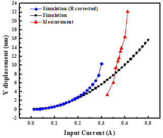
Fig 13 Measurement and simulation results of the center stage dispalcement in the Y direction.
Lastly, the breakage of the devices is shown in Fig 14. A mechanical failure was visible at the connecting hinge between the actuating chevrons and the displacement amplifying arm when the current was larger than 0.39A. To verify this breakage, the simulation result also showed that the stress was concentrated at the same location in which breakage was observed to occur. From the simulation result.
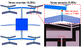
Fig 14. Overview and zoom-in of simulated stress results, as well as breakage micrograph in actual MEMS testing.
In conclusion, the measurement results of the MEMS device show a maximum displacement without breakage of 14 $\mu m$ abd is comparable to the maximum displacement result of 13 $\mu m$ from simulation results. No roation motion has been found during testing. And the location breakage of the structure can also be well predicted by the simulation.
Summary and Conclusion
In this research, a thermally-actuated 1 Degree-Of-Freedom translation nano-stage with displacement amplification schemes and a rotation-motion suppressing mirrored structure was designed and implemented. To control and read the stage position, a closed-loop feedback sensing and actuating circuit was designed in order to give the user a precise and consistent interface.
| MEMS Stage($\mu m^2$) | 500*500 |
| Max stage disp($\mu m$) | 14 |
| MEMS Sensitivity($fF/\mu m$) | 1.47 |
| $C_0(fF)$ | 349.575 |
| $\Delta C_{max}(fF)$ | 22.2 |
| Circuit Sensitivity($\mu V/fF$) | 3.5 |
| DAC Resolution | 8-bit(256 positions) |
| Controller Time Constant(ns) | 7.14 |
| Core Area(mm) | 1.34*1.34 |
Further imporvement
Becuase of limited time as well as strict rules for design and fabrication, the nano-stage can read position and correct the position by controller. More features can be added into the system including Noise measurement to improve position readiing accuracy. Disturbance might be a problem during moving, which might bring external force into the subject. Specific mechanical design might be needed if the disturbance affects the system largely. Besides, amplification structure can be further improved.Without strict design rules regulation, the 1 DOF system can also further develop into 2 DOF or more direction of movement.
Update Block Digram later
Reference
[1] M. Epitaux, J.-M. Verdeil, Y. Pétremand, W. Noell, and N. F. De Rooij,”Micro-machined XY stage for fiber optics module alignment,” in OpticalFiber Communication Conference, 2005: Optical Society of America, p.OThD2.
[2] K. Takahashi, “An optical lens scanner with electrostatic comb drive XYstage,” optical MEMS 2004, 2004.
[3] K. Takahashi, M. Mita, H. Fujita, and H. Toshiyoshi, “A high fill-factor comb-driven XY-stage with topological layer switch architecture,” IEICE Electronics Express, vol. 3, no. 9, pp. 197-202, 2006.
[4] P.-F. Indermuehle, C. Linder, J. Brugger, V. Jaecklin, and N. De Rooij, “Design and fabrication of an overhanging xy-microactuator with integrated tip for scanning surface profiling,” Sensors and Actuators A: Physical, vol. 43, no. 1-3, pp. 346-350, 1994.
[5] P.-F. Indermühle, V. Jaecklin, J. Brugger, C. Linder, N. De Rooij, and M.Binggeli, “AFM imaging with an xy-micropositioner with integrated tip,” Sensors and Actuators A: Physical, vol. 47, no. 1-3, pp. 562-565, 1995.
[6] Y. Sun, B. J. Nelson, D. P. Potasek, and E. Enikov, “A bulk microfabricated multi-axis capacitive cellular force sensor using transverse comb drives,” Journal of Micromechanics and Microengineering, vol. 12, no. 6, p. 832, 2002.
[7] Y. Sun, D. Piyabongkarn, A. Sezen, B. Nelson, and R. Rajamani, “A highaspect-ratio two-axis electrostatic microactuator with extended travel range,” Sensors and Actuators A: Physical, vol. 102, no. 1-2, pp. 49-60, 2002.
[8] C.-H. Kim, H.-M. Jeong, J.-U. Jeon, and Y.-K. Kim, “Silicon micro XYstage with a large area shuttle and no-etching holes for SPM-based data storage,” Journal of Microelectromechanical Systems, vol. 12, no. 4, pp. 470-478, 2003.
[9] J. Choi, H.-S. Park, K.-Y. Kim, and J.-U. Jeon, “Electromagnetic micro xy stage with very thick Cu coil for probe-based mass data storage device,” in Smart Structures and Materials 2001: Smart Electronics and MEMS, 2001, vol. 4334: SPIE, pp. 363-371.
[10] Y. Lu et al., “Design, fabrication and control of a micro XY stage with large ultra-thin film recoding media platform,” in Proc. IEEE/ASME Int. Conf. Adv. Intell. Mechatronics, 2005, pp. 24-28.
[11] J. Dong, D. Mukhopadhyay, and P. M. Ferreira, “Design, fabrication and testing of a silicon-on-insulator (SOI) MEMS parallel kinematics XY stage,” Journal of micromechanics and microengineering, vol. 17, no. 6, p. 1154, 2007.
[12] C.-T. Wu and W. Hsu, “An electro-thermally driven microactuator with two dimensional motion,” Microsystem technologies, vol. 8, no. 1, pp. 47-50, 2002.
[13] Q. Yao, P. M. Ferreira, and D. Mukhopadhyay, “Development of a novel piezo-driven parallel-kinematics single crystal silicon micropositioning XY stage,” in Smart Sensors, Actuators, and MEMS II, 2005, vol. 5836:SPIE, pp. 56-66.
[14] Lemkin M, Boser B E. A micromachined fully differential lateral accelerometer[C]. Custom Integrated Circuits Conference, 1996., Proceedings of the IEEE 1996. IEEE, 1996: 315-318.