
Instructor: Prof. Euisik Yoon from University of Michigan
Duration: 05/2022-08/2022
Introduction
Neural probes play an important role in medical and clinical application. With the help of neural probes, neuroscientists are able to know more about different brain regions and encode the signal of the brain. Hybrid system of neural probes and circuits is one of the important ways to make a neural probes system. However, as recording sites increased, it is challenging to electrically connect between flexible probes and ASICs and PCB.
Among all electrical connection techniques, flip-chip bonding is a commonly used method including bonding with anisotropic conductive films (ACF) etc. [1] </a > < a id = ``ref1'' > </a > However, ACF needs high temperature, high pressure, and high cost to fabricate. Therefore, developing a feasible, reliable, and high-throughput method to bond flexible probe and CMOS circuits together is necessary. There are a few prospective methods such as inkjet printing. [2] nkjet is gaining importance due to the ease of deposition on 3D and high resolution, which is a potential bonding method for hybrid integration of flexible probe and CMOS circuits. By introducing inkjet printing, the throughput of bonding would be greatly improved.
This project aims to use an Inkjet printer(Dimatix DMP2831) to connect the pads of a flexible probe to ASIC and/or PCB. By printing silver ink(SuntronicEMD 5730, conductive ink) on probe's pads and ASIC/PCB's pads, electrical connection is made between two components. One thing to point out is that the probe's pads and ASIC/PCB's pads are aligned in advance. As the printing doesn't require high temperature and high pressure, the 3D printing techniques has an advantage over the other methods with fine pitch and high throughput.
Experiment & Result
Process
- Align flexible probe's pads and ASIC/PCB's pads
- Fill cartridge with enough conductive ink
- Draw corresponding patterns same as pads
- Calibrate printing origin of the printer and calibrate theta
- Inkjet print ink on the substrate after setting printing origin and patterns
- Sinter the ink under high temperature(150-250℃) for some time
- Check printing results under microscope
Results
After many times of testing, two main problems appear during printing: leakage and misalignment.
Leakage
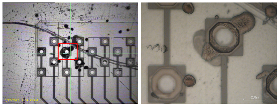
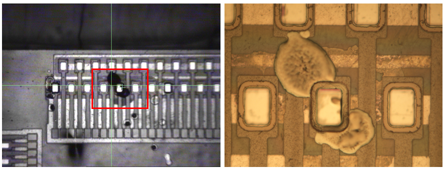
Fig 1. - Printing results taken in inkjet printing camera and microscope. Samples are printed on two types of cables: cable on silicon with aluminum deposited and cables on mockup.
According to the above results, instead of forming a drop on the pads, the ink leaks underneath the cables and probes because of surface tension force.
Several solutions have been tried while all solutions failed for different reasons:
Solution1: Change the way how to place cable and wafer/mockup by using water or IPA with/without baking for better attachment.
Results1: Cables might fold during alignment process and water or IPA with/without baking can not attach well enough with substrate. There's always gap between cable and substrate.
Solution2: Increase the substrate temperature and accelerate evaporate rate before liquid start to expand.
Result2: The ink still leaked at the 60℃, the highest substrate temperature. 30, 45℃ has also been tested but leakage still existed. It's because the sinter temperature is far higher than 60℃. What's worse, higher substrate temperature has a bad effect on cartridge nozzles, making easier to clog.
Solution3: flip the cable might help block ink leak by using metal ring.
Result3: Failed because there might still a large gap between cable and substrate.
Solution4: flip chip bonding the probes and substrates with 200N
Result4: and leakage became more severe after flip chip bonding.
There are also other potential solution for the problem while they also have some problems with them.
- Solution1: Solder ball printing(shown in Fig 3.) [3]
Concern: It needs electronic grade coating is needed which affects negatively the PCB/ASIC later. It also have high requirement on alignment and have concern in leakage.
- Solution2: Use a high viscosity ink
Concern: The leakage problem might exist and the ink is not capable with the Samba cartridge(a new type of cartridge for the tool)
- Solution3: Plasma processing
- Concern: plasma processing will also increase the surface wettability, which might help ink leak.
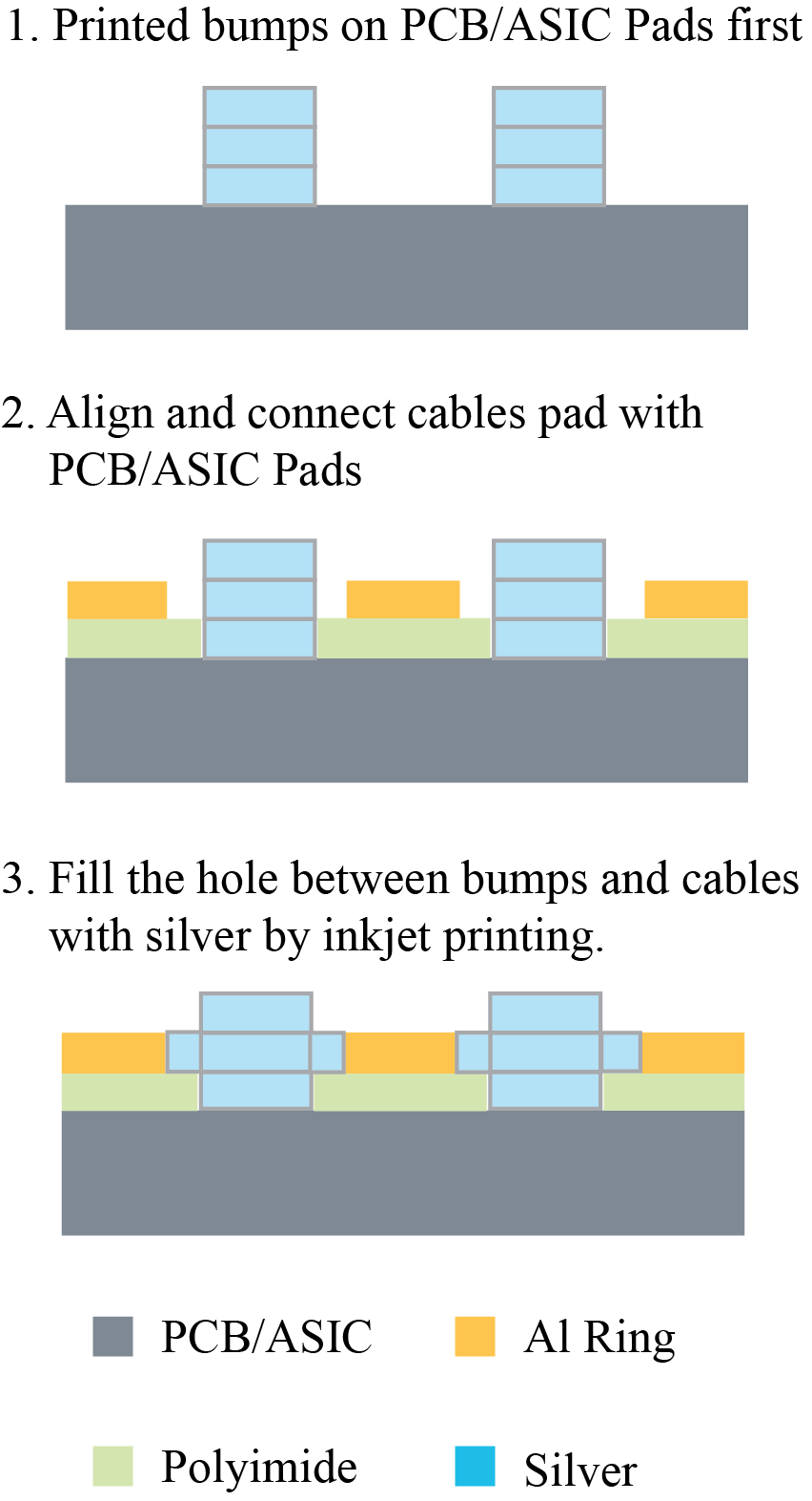
Fig 3. - Siver-bumps based fabrication process
Misalignment
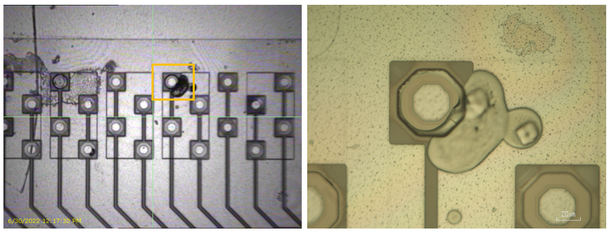
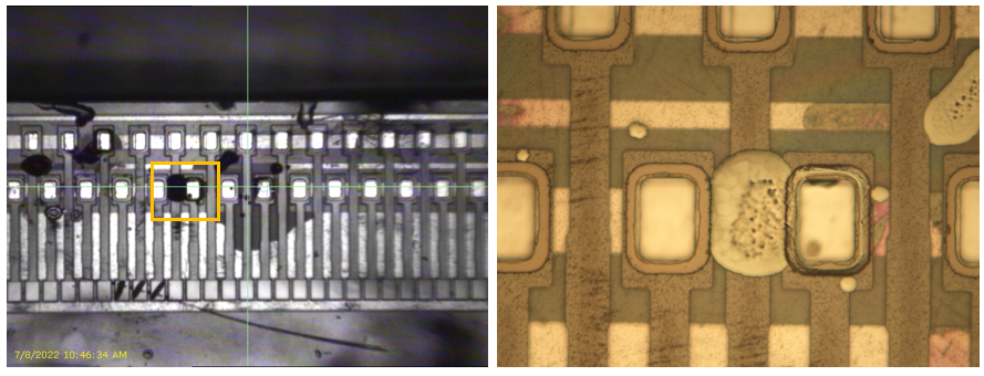
Fig 2. - Printing results taken in inkjet printing camera and microscope. Samples are printed on two types of cables: cable on silicon with aluminum deposited and cables on mockup.
The misalignment happens for a few reasons: Cartridge instability
- The cartridge can only be used in 2-3 weeks.
With too little ink in the cartridge, it will become very hard to control where it print. (~70 microns misalignment).
It's easy to clog if the substrate temperature increase while it is expected to increase the temperature to accelerate ink evaporation.
Tool Limitation
- The misalignment often happens in X direction.
The step of the motor of Y direction is much smaller than X direction: In X direction, 60μm movement is not reliable while Y direction can move to 10μm.
According to the manual, the repeatability of the printer: ± 25μm, negative on the alignment.
The printing origin can not remain the same place. Three different results have been received by using the same printing origin and same printing setting(voltage, temperature and nozzle to be used). The three results are in three different direction relative to printing origin while the nozzle work normally under drop watcher.
Conclusion
Every possible solution has been tried to save the projects but leakage is an unavoidable physics problem in the project. So the project is unfortunately wrapped up at this point.
Reference
[1] Park, S. Y., Na, K., Voroslakos, M., Song, H., Slager, N., Oh, S., Seymour, J., Buzsaki, G.; Yoon, E. (2022). A Miniaturized 256-Channel Neural Recording Interface with Area-Efficient Hybrid Integration of Flexible Probes and CMOS Integrated Circuits. IEEE Transactions on Biomedical Engineering, 69(1), 334–346. https://doi.org/10.1109/TBME.2021.3093542
[2] Nittala, P. V. K., Haridas, K., Nigam, S., Tasneem, S., & Sen, P. (2021). Characterization and optimization of bonding and interconnect technology for 3D stacking thin dies. Journal of Vacuum Science & Technology B, 39(5), 052207. https://doi.org/10.1116/6.0001160
[3] Shu, Z., Fechtig, M., Lombeck, F., Breitwieser, M., Zengerle, R., & Koltay, P. (2020). Direct Drop-on-Demand Printing of Molten Solder Bumps on ENIG Finishing at Ambient Conditions through StarJet Technology. IEEE Access. https://doi.org/10.1109/ACCESS.2020.3040035