
EECS413 Coursework Project
Duration: 11/2021-01/2021
Teammates: Haowen Chen, Zisu Wang
Introduction
An optical fiber operates at 5 Gbps. This project aims to design a CMOS wideband Transimpedance amplifier(TIA) that is capable of operating within a 5Gbps system. Lower bandwidth might cause pattern-dependent jitter and lower signal-to-noise ratio. It is also important to ensure gain high enough that input signals generate output levels exceeding the sensitivity of the limiting amplifier that follows the TIA.
Circuit Design
The 5Gbps optical system should have a maximum data frequency of 5Ghz and will require a TIA with at least 3.5Ghz bandwidth. This is to ensure minimum gain loss and distortion. As we learned in class, a single pole amplifier will continuously lose its gain with the increase of operation frequency. To define a range of operations, we used -3dB bandwidth and considered a 3dB gain reduction, and around -45 degree phase shift is acceptable.
The bandwidth of our amplifier will be limited by the dominant pole. Therefore, with a frequency lower than or slightly higher than the bandwidth, the amplifier will behave like a single pole system. This means our amplifier will maintain its DC gain until the bandwidth of 3.5Ghz, then drop off at a rate of 20db per decade until the second pole. At 5Ghz, this system will have a gain reduction around (5Ghz-3.5Ghz)/5Ghz / 10 Gainer-dec * 20dB-per-dec = 3dB. As discussed previously, -3dB gain reduction still provides high enough gain to maintain signal-to-noise ratio and low enough phase shift to avoid pattern-dependent jitter.
Overall Design
The general structure of our design is made up of three stages. The first part is a common gate amplifier which isolates the input capacitance from the photodiode while still providing high transimpedance. The second part is a series of common source amplifiers that maintains the high bandwidth of the common gate amplifier and provides good amplification. The third buffer is a common drain amplifier that acts as a voltage buffer to provide enough output voltage.
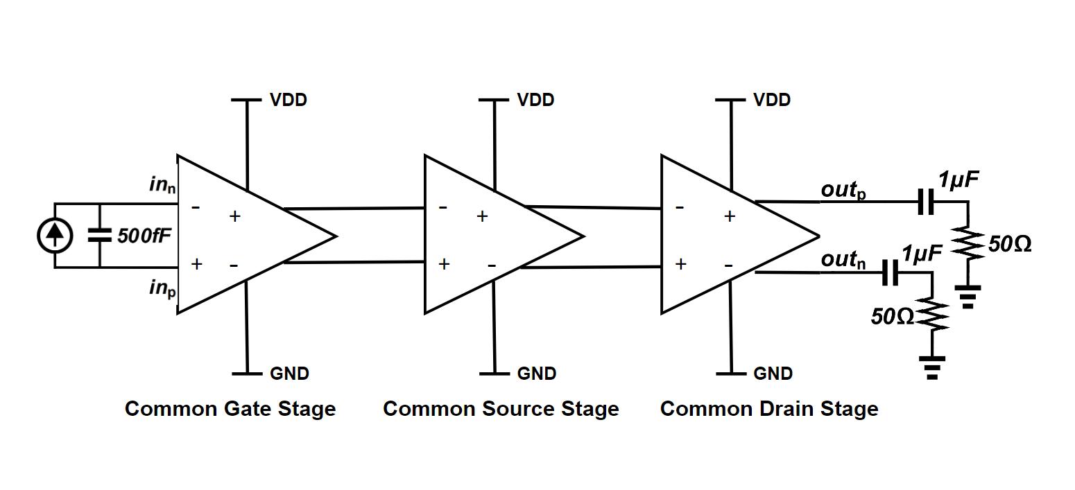
Fig 1. - General Structure of TIA
Common Gate Amplifier
In order to tolerate the high input capacitance as well as transforming the current input to voltage output, the frontend of the circuit was designed to be a common gate (CG) amplifier. The basic common gate amplifier structure is shown below.
$\tau_{in} = C_{gs}(R_{sig} \| 1/g_m)$
$\tau_{out}=(C_{gd}+C_L)R_L$
$A_v = g_m R_D$
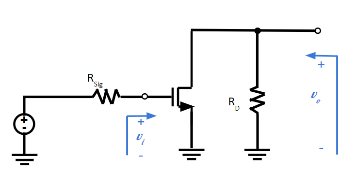
Fig 2. - Basic Common Gate Amplifier General Structure
One of the problems when designing is finding the balance between the gain and bandwidth, while preventing forming a dominant pole between the CG amplifier and the next stage, the load resistance has to be relatively low. Therefore, the gain $g_m$ as well as the dimension of the transistor has to be high.
The final common gate amplifier structure is shown in Fig 3. below. The CG amplifier(M1) uses a CS stage NMOS(M2) in replacement of the $R_{sig}$, in order to transform current input to voltage input and block the large pole from the 500fF input capacitance.A current mirror is built for the M1 and M2, reducing the difficulty of biasing. A resistor($R1_b$) in the structure below is used to design $I_{ref}$ for the stage. Finally, an inductor is introduced in series with M2, and in parallel with the input capacitance, forming a RLC loop for higher bandwidth.
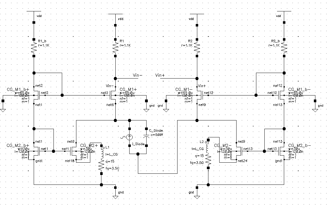
Fig 3. - Final Topology of the Common Gate Amplifier
Common Source Amplifier
Aiming to further enhance circuit gain in high frequency response, resistively loaded NMOS differential common source (CS) pairs have been applied as second part. The gain function of the differential amplifier is identical to the transfer function of the half circuit, which is the basic CS Amplifier shown in Fig 4. Tracking the signal from input to output. The following equation could be obtained. Under the restriction for frequency response and output voltage, $R_D$ and $\frac{W}{L}$ are carefully selected as high as possible.
$v_{in}=v_{sig}$
$v_{gs}=v_{i}$
$v_{o}=-g_m v_{sig} R_D$
$A_{vo} \equiv \frac{v_o}{v_i}=-g_m R_D$
$R_o=R_D$
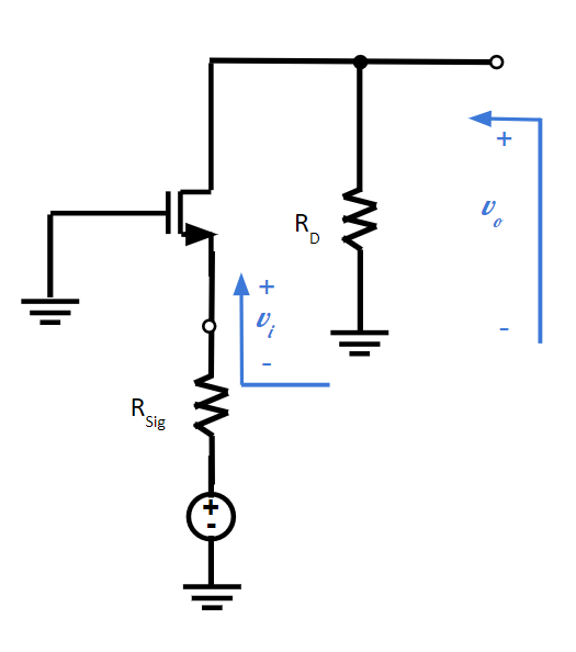
Fig 4. - Basic Common Source Amplifier General Structure
Thus, In the differential configuration of this CS stage, a CS NMOS (M2) is introduced as the current source, and a current mirror is built using M2_b and a resistor ($R_b$) to bias M2, providing desired $I_d$ for the CS amplifier stage. The $I_{ref}$ for this stage is defined by $R_b$ , and the current between the biasing branch ($I_b$) and main branch ($I_d$) is determined by the size ratio of M2_b and M2 shown in the following equation.
$\frac{W_{2b}}{W_2}=\frac{I_{ref}}{I_d}$
In this project, the ratio is set to be5 based on the following: $I_d$ enough for a high gain $g_m$ from M1, resulting in higher gain; and $I_{ref}$ can be relatively small to prevent large energy loss on the biasing resistor.
Two cascaded CS stages are needed to obtain enough gain. However, bandwidth will witness a tradeoff at this point. While the GBW (gain-bandwidth product) maintains the same, the feedback resistance is connected between two cascade CS amplifiers to reach the desired bandwidth. To further increase the bandwidth, an inductor is introduced to the load of one stage. During testing, a larger gain is observed from the second stage (of two cascading stages), indicating a larger pole at its output. Therefore, the inductor is chosen to be placed at the second CS stage. The final topology of the entire 2nd stage is shown in Figure 5., and a detailed schematic of a single stage is shown in Figure 6.
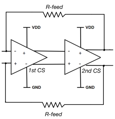
Fig 5. - Final Topology of the 2nd stage
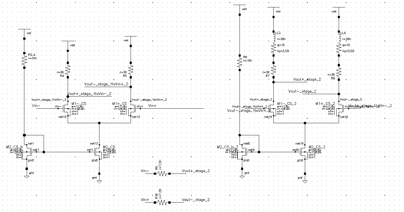
Fig 6. - Detailed Schematic of Common Source Amplifier Stage
Common Drain Amplifier
The third stage is a common drain stage. It isolates the previous stages from directly connecting to the load, preventing its performance from being influenced during application. Tt also transforms the high output impedance from the second stage (amplifying stage) to an impedance matching the transmission line, which is 50 ohms.
Last stage and $R_{source}$ act as the current mirror provides the desired $I_d$ for two stages. $R_{source}$ provides $I_{ref}$ for the third stage. Since $V_b$ doesn't significantly change, $I_{ref}$ remains similar. One of the important aspects to consider is the output impedance. The ratio of $I_{ref}$ and $I_d$ is determined by the size of $M_{1b}$ and $M_1$.
$I_{ref}=\frac{(V_{dd}-V_b)}{R_{source}}$
$R_{out}=(g_{m1}+g_{ds1}+g_{ds2})^{-1}$
$I_{ref}/I_d=W_{1b}/W_1$
The final design is shown in Fig 7. The final output impedance is $42 \Omega$.
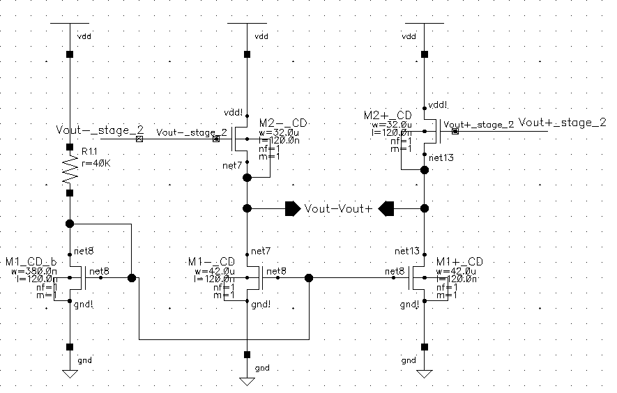
Fig 7. - Detailed Schematic of Common Drain Amplifier Stage
Simulation Result and Analysis
To evaluate the system, different simulation have been made in the project.
Power Dissipation
The power dissipation of the circuit was maintained at 24.4515 mW in the frequency range of 1 MHz to 10 GHz is shown in Figure 8.
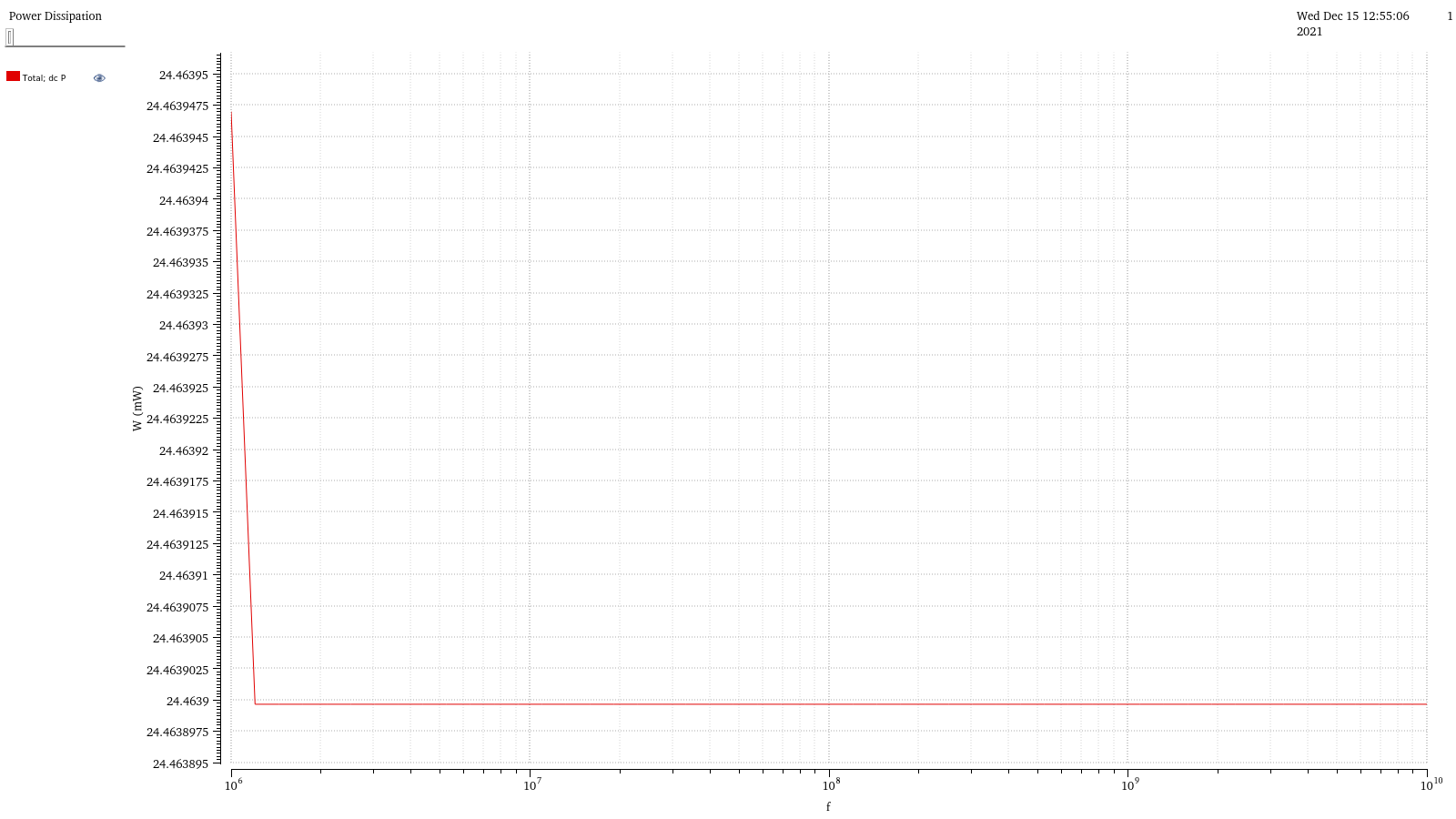
Fig 8. - Power Dissipation Analysis
Transimpedance
By setting the AC current magnitude as 1A and running the AC analysis in the frequency range of 1 MHz to 10 GHz, the transimpedance of the circuit was shown to be $2.5096K\Omega$ in Fig 9.
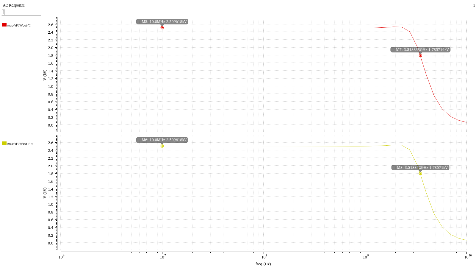
Fig 9. - AC Analysis in Frequency Range of 1M to 10G
Bandwidth
In the frequency range from 1 MHz to 10 GHz, the AC response spectre in dB20 scale was shown to be 3.5013GHz.
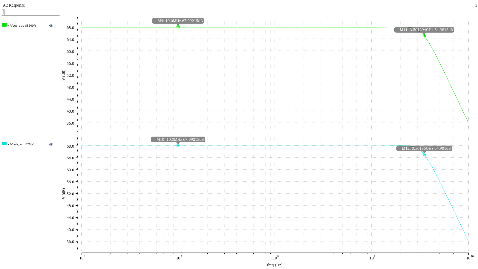
Fig 9. - 20dB Plot of Output in AC Analysis
Differential Output Swing
In the transient Analysis, the differential swing of the transimpedance amplifier for + and - output is 141.163mV and 142.771mV respectively.
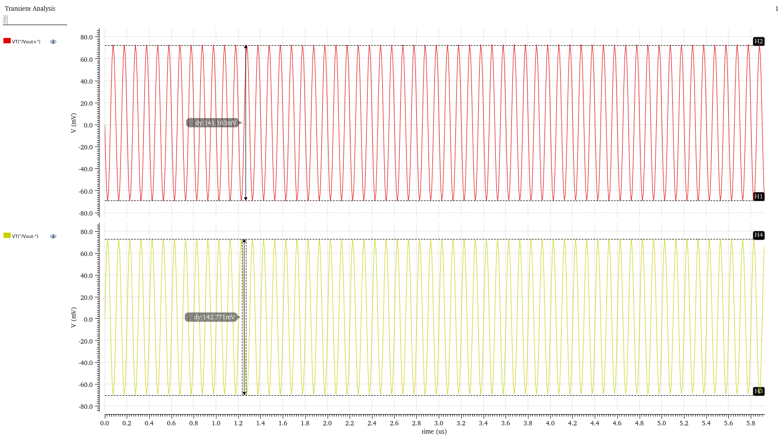
Fig 9. - Transient Analysis with Input Amplitude of $29.8 \mu A$ at $10 MHz$
Diffeerential Output Slew Rate
The slew rate of the differential amplifier is calculated to be:
$(132.226mV+128.839mV)/228.503ps=1.143V/ns$
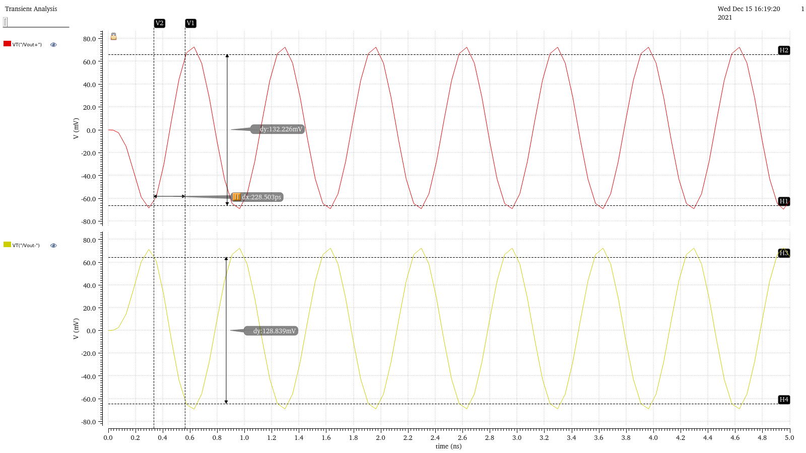
Fig 9. - Transient Analysis with Input Amplitude of $28.6 \mu A$ at $1.5GHz$
Conclusion
In this project we design a high-bandwidth and high-gain Transimpedance Amplifier for 5Gbpas final operating system. Following table shows design specs of the system.
| DC Power Dissipation | 24.4515 mW |
| Transimpedance | 2.5096 $k\Omega$(for single differential output vs. photodiode current) |
| ~3dB Bandwidth | 3.5013GHz |
| Differential output Swing | 141.163mV and 142.771mV |
| Differential output slew rate | 1.143V/ns |
| Total chip size | 465$\mu m$ * 214$\mu m$ |