
Title: Microsystem Design
Author: Stephen D. Senturia
Duration: 07/2022-present
Chapter 1 Introduction
What's in a name?...A rose by any other name would smell as sweet.
-- W. Shakespeare in Romeo and Juliet
1.1 Microsystems vs. MEMS
1.1.1 What are they?
"Microelectromechnical systems(MEMS)": micro establishes a dimensional scale, electro suggests either electricity or electronics(or both), and mechanical suggests moving parts of some kind. But the concept has gown to encompass many other types of small things including thermal, magnetic. fludic, and optical devices and systems, with or without moving parts.
In general, MEMS share several common features:
MEMS involve both electronic and non-electronic elecments, and perform functions that can include signal acquisition(sensing), signal processing, actuation, display, and control. (performing chemical and biochemical reactions and assays)
System issues including packaging, system partitioning into componens, calibration, signal -to-noise ratio, stability, and reliability must be confronted.
The most successful MEMS have been those which involve paradigm shifts from the "macro" way of doing things. Great examples are inkjet print head, thin-film magnetic disk heads and microfluidic devices.
Some MEMS involve large arrays of microfabricated elements, such as uncooled ingrared imaging devices.
1.1.2 How are they made?
"micromachining": Lithographic techiniques require flat susbstrates. Silicon is often used. Lithography offers in-place sub-micron precision on dimension scales from micron and milimeter. Thin-fillm deposition and etching techiniques in combination with wafer-bonding techniques allow patterning of the third dimension. Integrated circuits and partition the microsystem into susbsystems are two ways to build the system. Encapsulation and packaging of the components into a system impact the design too.
1.1.3 What are they made of?
The choice of materials is determined by microfabrication constraint. Most of these are inorganic materials, including silicon, silicon dioxide, silicon nitride, aluminum and tunsten. Certain polymer might be use as well.
Certain properties are critical in device performance, for examplt, the elastic modulus or residual stress of a suspended beam.
1.1.4 How are they designed?
On one level, the designer mush documen the need and specificaiton for a proposed microsystem. At another level, for each proposed approach, one must deal with details of partitioning the system into components, materials selection and the responding fabrication sequences for each componen, methods for packaging and assembly.
Quantitive models play a key role in the design process.(perdiction, troubleshooting, evalution)
1.2 Markets for Microsystems and MEMS
Forecasting is difficult. expecially the future.
-- Chinese forture cookies
1.3 Case Studies
| Case Study | Partitioning | Technology | Transduction | Packaging |
|---|---|---|---|---|
| Pressure Sensor | Monolithic | Bulk micromachining with bipolar circuitry plus glass frit wafer bongnig | Piezoresistive sensing of diaphram deflection | Plastic |
| Accelerometer | Monolithic | Surface micromachining with CMOS circuitry | Capacitive detection of proofmass motion | Metal can |
| Resonant Rate Gyroscope | Hybrid | Bulk micromachined quatz | Piezoelectric sensing of rotation-induced excitation of resonant mode | Metal can |
| Electrostatically Driven Display | Hybrid | Surface micromachining using XeF2 release | Electrostatic actuation of suspended tensile ribbons | Bonded glass device cap plus direct wire bond to ASIC |
| DNA Amplification with PCR | Hybrid | Bongded etched glass | Pressure-driven flow across temperature-controlled zones | Microcapillaries attached with adhesive |
| Catalytic Combustible Gas Sensor | Hybrid | Surface micromachined with selective deposition of catalyst | Resistance change due to heat of reaction of combustible gas | Custom mounting for research use |
Table 1.2 Summary of the Case Studies examined in this book
Chapter 2 An Approach To MEMS Design
If technology-driven design is a hammer looking for a nail, then markei-driven design is a nail looking for a hammer. A good designer will match hammers to nails, regardless of which comes first.
- Anonymous
2.1 Design: The Big Picture
Examine the big picture, including difficult subhects such as creativity and invention, market opportunities, and choices of technologies, system architectures, and manufacturing methods.
2.1.1 Device Categories
Technology Demonstrations: small numbers of working devices are needed to test a device concept or push the capabilities and limits of a particular fabrication technology.(require only a handful of working devices. Device-todevice consistency is not usually important.)
Research Tools: components or fully systems have the porpose of performing a highly specialized task. (must typically be calibrated, and should have repeatable behavior.)
Commercial Products:The numbers of working devices and the degree of precision and accuracy needed depend on the market.(Device-todevice consistency and high manufacturing yield are likely to be of paramount importance.)
2.1.2 High-Level Design Issues
- Market: need? How large is the market? How fast will it develop?
- Impact: Paradigm shifts?
- Competition: Equivalent product
- Technology: Make and package the product available in-house or must be acquired through vendor?
- Manufacturing: acceptable cost
Different product has different priority.
| Category | Markets | Impact | Competition | Technology | Manufacturing |
|---|---|---|---|---|---|
| Technology Demonstration | ++ | +++ | |||
| Research Tools | ++ | ++ | + | +++ | ++ |
| Commercial Products | +++ | +++ | +++ | +++ | +++ |
Table 2.1 Relative Importance of High-Level Design Issues
2.2 Modeling Levels
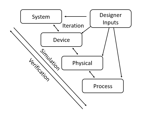
Fig.2.2 - Different modelings levels for microsystems.
At the top is the system level. A coupled set of ordinary differential equations (ODE's) to describe the dynamical behavior of the system(block-diagram descriptions and lumped-element circuit models), often written in a coupled set of first-order ordinary differential equations for the state variables of the system.
At the bottom is the process level. This is where the process sequence and photomask designs for device manufacture are created. (CAD & TCAD)
The physical level addresses the behavior of real devices in the threedimensional continuum. The governing equations are typically partial differential equations (PDE's).
At device level, create what are called macro-models or reduced-order models in a form that captures the essential physical behavior of a component of the system, and simultaneously is directly compatible with a system-level description.
2.2.1 Analytical or Numerical?
- SIMULINK for system-level modeling
- MATLAB for selected numerical device-level and physical-level simulation
Important block diagram can be referred.
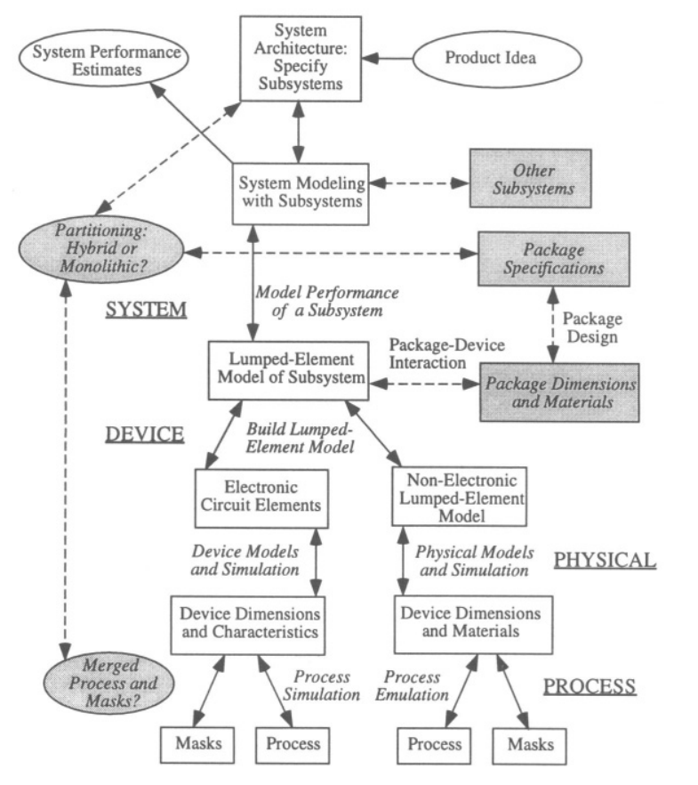
Fig.2.3 - Expanded view of the "Modeling and Analysis" block.
2.4 Going Forward From Here
Developing the analysis tools to assist in (1) the assessment of different device designs and their relative performance and (2) the prediction of performance (in great detail) for the design ultimately selected. The following issues are concerned:
- System Architecture: microfabricaed components, electronics and the package
- System Partitioning: how affect packaging?
- Transduction Methods: variations that would improve performance or reduce cost
- Domain-Specific Knowledge: devices typically involve at least two energy domains(laws of physics and chemitry)
- Electronics: Interface between physical device and electronic part of the system; device noise
Chapter 3 Introduction
In small Propoertions we just beauties see;
And in short measures, life may perfect be.-- Ben Jonson
3.2 Wafer-level Processes
3.2.1 Substrates
- single-crystal silicon
- single-crystal quartz
- glass
- fused (amorphous) quartz
3.2.1.1 Silicon Wafers
Single-crystal-silicon wafers are classified by the orientation of the surface relative to the crystalline axes. The nomenclature is based on the Miller indices. Silicon is a cubic material, constructed from two interpenetrating face-centered cubic lattices of atoms.
The complete silicon unit cell is whon in Fig. 3.1. Every atom is tetrahedrally bonded to four neighbors. The illustration on the left shows an interior atom bound to one corner atom and three face-center atoms(every atom is identical). atom in (111) surface is tetrahedrally bonded to three atoms while atoms on (110) or (100) surfaces are tetrahhedrally bonded to only two atoms beneath the surface, have two potential "dangling" bonds. The difference in bonding of the atoms on the different crystal surfaces make certain etchants etch anisotrpically.
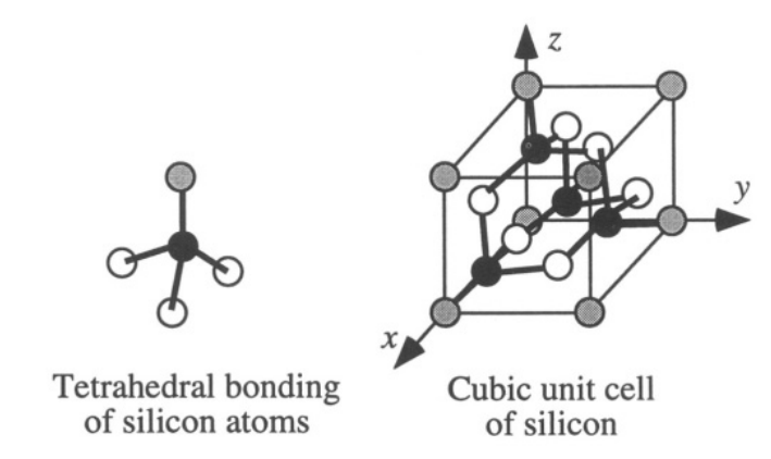
Fig 3.1. - The tetrahedral bonding of each atom in the silicon unit cell and Cubic unit cell of silicon.
Most silicon crystals are grown from a highly purified melt using the Czochralski method(CZ). A small seed crystal with a preselected orientation is inserted into a heated crucible containing a highly purified melt. The seed is gradually pulled out of the melt while the crucible containing the melt is rotated. The melt temperature and pulling speed are controlled to balance crystal growth rate with pulling rate. The schematic of the principle of the Czochralski method is shown in Fig 3.2.
An alternative method is called float zone(FZ). Starting with a polysilicon rod, a radio-frequency heater creates a local melted zone that is dragged from one end of the rod to the other. To start the growth, a seed crystal can be used at one end of the rod assembly.
Chemical impurities and structural imperfections(point defects, dislocations) specify the quality of silicon crystals. CZ wafers typically have higher amounts of residual chemical impurities, such as carbon, oxygen and heavy metals, compared to FZ wafers because the molten zone tends to carry impurities with it as it sweeps from one end of the rod to the other. However, sometimes it has benefit in certain microelectronic device as the presence of oxygen promotes the migration of point defects during high-temperature process. The higher purity FZ wafers, on the other hand, have requirement of heavy-matal contamination and dislocation.
Wafers are supplied in standard diameters and thicknesses, and are polished to mirror smoothness on either one or both sides.
Wafers are also characterized by their doping level, n-type or p-type. Dopants are added to the starting melt in order to incorporated uniformly as the crystal grows in CZ crystal growth. Different crystal surface have differnt patterns fo flat edges. Fig. 3.3 show how relative orientation of the secondary wafer flat to thhe larger primary wafer flat provides the identification.
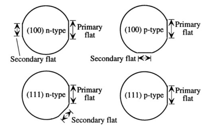
Fig 3.2. - Primary and secondary wafer flat are used to identify orientation and types.
3.2.1.2 Quartz Wafers
Quartz is a hexagonal material, with the z-axis conventionally identified as the hexagonal axis. Because of its piezoelectric properties, single-crystal quartz plays an important role in MEMS. Different from silicon wafer, the standard nomenclature for single-crystal quartz substrates is not based on Miller indices. The basic orientations, such as X-cut and Z-cut quartz, refer to the crystalline axes normal to the plane of the wafer, but AT-cut quartz refer to off-axis orientations that are selected for specific temperature insensitivities fo thir piezoelectric or mechanical properties.
3.2.2 Wafer Cleaning
The standard set of wafer cleaning steps is called the RCA cleans
1. The standard set of wafer cleaning steps is called the RCA cleans (a 7:3 mixture of concentrated sulfuric acid and hydrogen peroxide, "pirhana")
2. Organic residues are removed in a 5:1:1 mixture of water, hydrogen peroxide, and ammonium hydroxide. Oxide will grow on silicon in this step so dilute HF etch should be inserted to remove the oxide.
3. ionic contaminants are removed with a 6:1:1 mixture of water, hydrochloric acid, and hydrogen peroxide.
No metallic cations should be contained in the cleaning solutions. The RCA cleans must be performed before every high-temperature step(oxidation, diffusion, or chemical vapor deposition).
3.2.3 Oxidation of Silicon
The oxidation reaction is stratghtforward: oxegen reacts directly with the silicon, forming silicon dioxide. The dependence of oxidation rate on oxide thickness has been captured in the Deal-Grove model of oxidation kinetics.
If $x_i$ is the initial oxide thickness present on the wafer, then the final oxide thickness $x_f$ is given by
$x_f=0.5A_{DG}[\sqrt{1+\frac{4B_{DG}}{A^2_{DG}}(t+\tau_{DG})}-1]$
where $A_{DG}$ and $B_{DG}$ are temperature-dependent constants, $t$ is the oxidation time, and $\tau_{DG}$ is given by
$\tau_{DG}=\frac{x^2_i}{B_{DG}}+\frac{x_i}{B_{DG}/A_{DG}}$
There are two asymptotic regions. At short times, the square root can be expanded to yield the linear rate model:
$x_f=\frac{B_{DG}}{A_{DG}}(t+\tau_{DG})$
At long times. parabolic rate model is obtained:
$x_f=\sqrt{B_{DG}t}$
Overall, about 54% of the total oxide thicknes appears as add thickness. The remaining 46% is conversion of substrate material to oxde. Fig 3.3. shows the consumption.
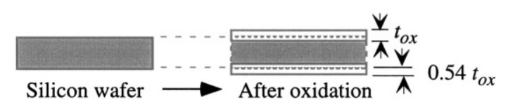
Fig 3.3. - Thermal oxidation consumes some of the wafer thickness.
The diffusion rate of oxygen through oxide can be significantly enhanced if there is water vapor present. It is because water breaks a silicon-oxygen-silicon bond, which is more mobile than molecular oxygen.Hense, the oxidation rate is faster. However, dry oxidation is typically used whtn the highest-quality oxides are required.
3.2.4 Local Oxidation
When a portion of a silicon wafer is covered with an oxygen diffusion barrier, such as silicon nitride, oxidation cannot occur. As a result, protected regions of a wafer remain at their original heights, while unprotected regions are converted to oxide. Stress are generated at its edges, creating a tapered oxide called a bird's beak The $LOCOS$ or $Local \ Oxidation$ isolate individual transistors and interconnecting them without creating parasitic transistors beneath the interconnections.
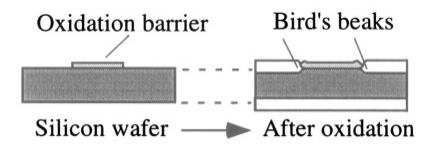
Fig 3.4. - Bird's beaks and its formation are shown in the fig.
3.2.5 Doping
There are two types of dopants: p-type(holes) and n-tpe(electrons). When a region contains dopants of both types, it is the net dopant concentration in a region that determines its conductivity type, which means an initially p-type regin can be converted to an n-type region by adding more n-type dopant than p-type dopand amount(counter-doping). The process of doping consisstes of two steps: deposition and drive-in
3.2.5.1 Ion Implantation
Ion implantation is a process in which a particle accelerator shoots a beam of dopant atoms directly into the wafer. The dopant atoms stay at a particular depth into the substrate, which is called projected range. The depth depends on the ion energy, the ion species, and the material into which the implantation is performed.
The fact that ion implantation has a finite range means that surface layers can be used to mask regions of the wafer, preventing the dopant ion from reaching the wafer. Photoresist, silicon dioxide or silicon nitride are commonly used as implant masks.
Because direct ion bombardment into a surface can knock surface atoms loose (sputtering), it is normal to do ion implantation through a thin protective layer, such as a few tens of nm of silicon dioxide. This oxide also tends to scatter the ions slightly as they pass through, providing a range of impact angles into the silicon(channeling). The presence of the oxide layer affects the penetration depth into the substrate, and must be taken into account.
3.2.5.2 Drive-In Diffusion
Ion implantation provides a certain dose of dopants in a layer near the silicon surface. To redistribute these dopants (as well as to remove any residual defects produced by the implantation process), high-temperature anneals with a protective oxide layer to prevent dopant evaporation in a suitable atmosphere are used. The process for redistribution is called diffusion Temperature affects the diffusion constants, and different dopants also have different temperature dependences.
y second-order effects that affect diffusion profiles. Boron can dissolve slowly into overlying oxide, slightly depleting the surface concentration. Diffusion rates are also affected by the presence of point defects and by other dopants. Whether or not oxidation is taking place during the drive-in also have influence in diffusion rates.
3.2.6 Thin-Film Deposition
Many microelectronic process steps involve the deposition and subsequent patterning of a thin film.
3.2.6.1 Physical Vapor Deposition
Physical vapor deposition(PVD), covers two major methods: evaporation, and sputtering.
Evapoaration is used primarily for metal and must be donw under high-vacuum. Evaporation with an e-beam is quite directional, allowing interesting shadowing effects to be used. Such method is used to deposit electrodes on the sides of etched quartz microstructures used in accelerometers and rate gyroscopes.
Sputtering is a process in which chemically inert atoms, such as argon, are ionized in a glow discharge (plasma). Thhe ions are accelerated into dark space and knocked out to reach the substrate. Sputtering takes palce in a low-pressure gas environment.
Though sputtering is less directional than e-beam evaporation, it typically can achieve much higher deposition rates. Therefore, it is the metallization method of choice in most microelectronic manufacturing.Sputtering can also be used with dielectric films, such as silicon dioxide. Some specialty materials, such as the piezoelectric film zinc oxide and aluminum nitride, are well-suited to sputtering.
3.2.6.2 Chemical Vapor Deposition
Chemical vapor deposition (CVD) is a chemical reaction occurs on the surface of the wafer resulting in deposition. CVD depositions are typically performed under low-pressure conditions (less than 1 Torr) and usually involve an inert diluent gas, such as nitrogen, in addition to the reacting species. LPCVD is a typical CVD type. However, the process goes through under high temperature. Thus, it is necessary to perform all CVD processes before any depositions with metals. However, Tungsten is able to withstand CVD temperatures.
Epitaxy: If CVD deposition occurs on a single-crystal substrate, it is possible for the underlying crystal to serve as a template for the deposited material to develop as an extension of the single crystal. It is widely used for III-V compounds.
- If at a given temperature, the deposition rate is slow enough to provide ample time for atoms to migrate along the surface and find equilibrium lattice sites, then epitaxy is possible.
- At higher deposition rates, the deposition occurs as polycrystalline material called polysilicon.
- If a portion of the single-crystal is exposes and the rest is covered with silicon dioxide, epitaxial growth can occur over the single-crystal while polisilicon is being posited over the oxide.
Deposition rates can be enhanced if the deposition occurs in a glow-discharge plasma. (PECVD) It used to deposit dielectric films at lower temperature. It is extremely important in constructing insulation layers for use with metallization.
The material properties can depend in detail on the exact process, including such issues as temperature, gas flow rates, pressures, and the chemistry or morphology of the layer on which the film is deposited.
3.2.6.3 Electrodeposition
Electrodeposition, or electroplating, is an electrochemical process in which metal ions in solution are deposited onto a substrate.
- Metals that are well suited for plating are gold, copper, chromium, nickel, and magnetic iron-nickel alloys (permalloy).
- Most plating involves control with an applied electric current.The uniformity depends on maintaining a uniform current density. Features of different areas, and regions at the corners of heatures, may plate at different rates.
- Plating is used in microelectronics to deposit coppoer interconnect and making high-aspect-ratio microstructures(HARM, LIGA).
3.2.6.4 Spin Casting
Thin films can be deposited from solution by a technique called spin casting.The material to be deposited, typically a polymer or chemical precursor to a polymer, is dissolved in a suitable solvent.
Spinning is the standard method for depositing photoresist, a photosensitive polymer layer used in photolithography.
3.2.6.5 Sol-Gel Deposition
Some materials, especially various oxides, can be formed from the sintering of a deposited gel layer that contains a suitable precursor. Spin-on glasses are examples of silicon dioxide deposited in this manner. It is also possible to deposit various piezoelectric materials, such as lead zirconate titanate (abbreviated PZT), by this method.
3.2.6.6 Thin Film Stress
A major problem with deposited thin films is the control of the state of mechanical stress. All deposited thin films have some degreee of in-plate stress and the stress distribution is sensitive to processing conditionss, and to subsequent thermal history such as post-deposition anneals.
3.2.7 Wafer Bonding
Wafer bonding is a method for firmly joining two wafers to create a stacked wafer layer.
3.2.7.1 Direct Wafer Bonding of Silicon
The direct bonding of silicon wafers to one another requires high temperatures, on the order of 1000°C.
- Cleaning and hydration of the surfaces to be bonded.(smooth and particle-free) Using hydrogen bonding of the hydrated surfaces is to provide a modest degree of adhesion.
- A variation on silicon-to-silicon bonding is that the bottom wafer has a thermal oxide on it. The surfaces are cleaned and hydrated, then contacted and annealed, and the top wafer is thinned.
- Bonding can also be done on patterned wafers. Piezoresistors can be made in this way,
3.2.7.2 Anodic Bonding
field-assisted bonding, or anodic bonding is related to the mobility of sodium ions in the glass. When the silicon wafer is placed on the glass, and the two are heated to temperatures on the order of 500°C, a positive voltage (300 - 700 V) applied to the silicon repels sodium ions from the glass surface, creating a net negative charge at the glass surface. The force of attraction between the positively charged silicon wafer and the negatively charged glass surface brings the two surfaces into intimate contact. As with silicon-to-silicon bonding, this bonding method is very susceptible to interference from particulate contaminants.
3.2.7.3 Bonding with an Intermediate Layer
Glass frits, which are powdered slurries of relatively low-melting glasses, can be applied selectively to parts of the surface of one of the wafers using techniques such as screen printing. After a low-temperature bake to reduce the fluid content of the frit layer, the wafers are contacted and annealed, flowing the glass into a continuous layer that bonds the wafers together. Gold layers are also another alternative. Polymic adhesives(polyimides, silicones, epoxy resins) can also be used, provided that the cleanliness and thermal requirements of the device process are not compromised.
3.3 Pattern Transfer
Pattern transfer consists of two parts:
- A photo-process
- Create the pattern: a chemical or physical process either moving or adding material.
3.3.1 Optical Lithography
- Photoresists, polymeric optically-sensitive materials(spin).
- Photomask contact or close procimity
- Ultraviolet light is directed through the mask onto the wafer, exposing the unprotected portions of the resist(chemical properties change).
- Nagative & Positive(protected region is stay) photoresist. "Positive resist protects."
- Contact lithograpthy: same size mask.
Projection step-and-repeat-lithography: reduced by factor. - Process biases and random patterning errors can result in variations in device performance that must be corrected with suitable calibration.
3.3.2 Design Rules
Misalignment at each step, robust process design calls for the minimum mandatory offsets. Design rules specify a minimum overlap between such mask features so that even in the worst expected misalignment, the fabricated structure is acceptable.
3.3.3 Mask Making
- Layout
- Optical pattern generator use a photographic emulsion on the quartz plate that becomes optically opaque when exposed and developed.
- Write pattern into an electron-beam resist.
3.3.3.1 Double-Sided Lithography
One first aligns the back-side mask to fiducial marks on the tool, then places the wafer over this mask, and aligns the wafer to the tool using alignment features on the front.
3.3.3.2 Soft Lithography
It uses a molded polymeric body(PDMS) to accomplish physical pattern transfer.
3.3.4 Wet Etching
Removing Material through the openings in a suitable masking layer.
3.3.4.1 Isotropic Wet Chemical Etching
- A suitable liquid chemical attacks the exposed region of the substrate and leaves the protected regions alone.
The rate of etching and the shape of the resulting etched feature depend on many things: the type of substrate, the specific chemistry of the etchant, the choice of masking layer (and the tightness of its adhesion to the substrate), the temperature (which controls reaction rates), and whether or not the solution is well stirred (which affects the rate of arrival of fresh reactants at the surface).
- reaction-rate controlled / mass-transfer-limited.
- Most wet etching is isotropic, not depending on orientations.
- If the materials underneath is etched, it referred to surface micromachining.
One significant technology problem in surface micromachining is the unintended adhesion of released mechanical elements to the substrate.
Stiction: When using a wet release etch, the surface tension during drying can pull compliant beams into contact with the substrate, and during the final drying, they can adhere firmly together.
Solution: the use of self-assembled molecular monolayers (SAM's) to coat the surfaces during the final rinse with a thin hydrophobic layer, reducing the attractive force;the use of vapor or dry-etching release methods(XeF2)
- various drying methods (freeze drying and drying with CO2)
temporary mechanical support of the moveable structure during release using posts of photoresist or some other easily removed material.
- Wet etching can also be used to etch deeply into the substrate.(bulk micromachining).
3.3.4.2 Anisotropic Wet Etching
The mechanisam responsible for orientation dependent etching in silicon is the detailed bond structure of the atoms that are revealed in different surface planes. As etching proceeds, the exposed {100} planes etch rapidly while the {111} planes etch slowly. Every {111} plane intersects a (100) surface along one of the <110> directions shown in Fig 3.5.. Hence, starting from every straight mask edge that is aligned with one of the <110> directions, a slow-etching {111} plane becomes revealed by the etch. It makes a 54.7° angle with the plane of the wafer, the characteristic feature of anisotropically etched bulk-micromachined structures.
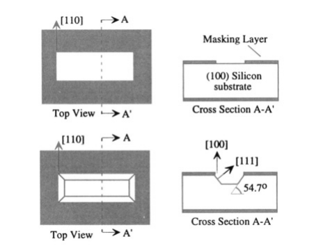

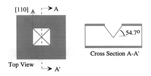
Fig 3.5. - When a (100) oriented wafer with mask features aligned to <110> directions is placed in an anisotropic etchant.{100} planes etch rapidly, but {111} plenes etch slowly.
This undercutting phenomenon extends to other shapes. Other typical etching samples also shown in Fig 3.6. Undercutting has important implications for alignment accuracy. The bounding rectangular etch pit is what determines the final etched shape.
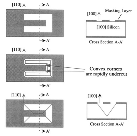
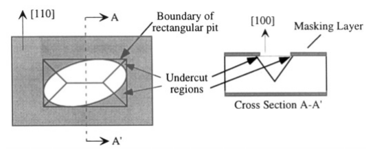
Fig 3.6. - Other examples of etching a (100) oriented wafer
3.3.4.3 Etch Stops for Wet Etching
- Electrochemical Etch Stop(Electrochemical passivatoin)
- When a silicon wafer is biased with a sufficiently large anodic potential relative to the etchant, it tends to oxidize.
- The oxide on the surface masks the etch.
- The use of this electrochemical property to control the thickness. The depth of the junction can be accurately controlled by the combination of ion implantation and drive in.
- p+ Etch Stop
If instead of using an n-type diffusion into a p-wafer, a heavily boron doped p+ layer is formed by ion implantation and diffusion, the anisotropic etch will terminate without requiring application of anodic bias.
- The etch-rate selectivity is not quite as high as for passivating oxides.
- Residual Tensile stress might affect the performance
- Dielectric Etch Stop
- Some layer is replaced by a material that is not etched, for example. silicon nitride
- No Etch Stop: Making Through Holes
If no etch stop is used, a hole is produced all the way through the wafer. The sloped sidewalls of the holes also offer an opportunity for making interconnects between the back and the front of a wafer.
3.3.5 Dry Etching
Chemically reactive vapors and the reactive species in glow-discharge plasmas are highly effective etchants. These are classified into two groups: vapor etching, and plasma-assisted etching.
3.3.5.1 Vapor Etching
$XeF_2$ is a highly selective vapor etchant for silicon. It is ideal for the dry release of surface micromachined structures in which polysilicon is used as the sacrificial layer.
3.3.5.2 Plasma-Assisted Etching
Ion Milling: The least selective use of ions produced in a plasma is for the sputtering away of material. Selectivity is achieved by the relative rate of sputtering of different materials.
A variant of this process is focused ion beam milling, using an argon ion source in combination with focusing electrodes so that ions from the plasma only strike the surface within a small region.
Ashing: When the ions have some chemical reactivity, such as the ions produced in an oxygen plasma, the result of reaction of the ionic species with the surface of the wafer can be a volatile species that is removed by the vacuum pump.
| Material to be etched | Etcha gas |
|---|---|
| Silicon or polysilicon | $CF_4$,$SF_6$ |
| Silicon dioxide | $CF_4/H_2$ |
| Silicon nitride | $CF_4/O_2$ |
| Organics | $O_2$, $O_2/CF_4$,$O_2/SF_6$ |
| Aluminum | $BCl_3$ |
The shape of a plasma-etched feature is a strong function of the etching conditions. The higher the base pressure in the plasma, the more isotropic the etch profile.
reactive ion etching at the limit of low pressures and a correspondingly high degree of directionality. Sidewalls are not significantly etched because the ions do not strike them.
Deep Reactive Ion Etching (DRIE): This process takes advantage of a side-effect of a glow discharge, the tendency to create polymeric species by chemical crosslinking.
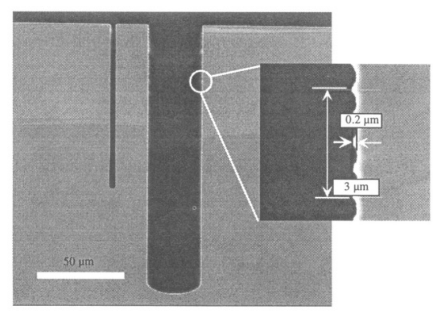
Fig 3.7. - Photo of features etched in silicon with DRIE.
3.3.6 Additive Processes: Lift-Off
lift-off: When metal is etched with patterns and the resist(photoresist and metal on it) is stripped, the matal on top of the resist is "lifted-off"</p>
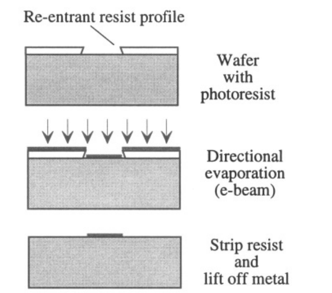
Fig 3.8. - Lift-off for patterning evaporated metals.
It exploits the deposition of the evaporated metal onto the edges of the masking layer, gradually closing off the opening.The evaporated layer at the substrate becomes conical in shape, finally reaching a sharp point when the masking layer closes off completely.(Spindt Process)
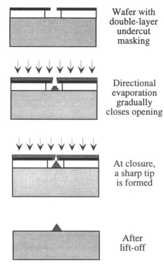
Fig 3.9. - The use of a midified lift-off process to create sharp tips.
### 3.3.7 Planarization There are three primary difficulties with non-planar surfaces:etching processes can leave behind unetched "stringers" non-planar wafers cannot be successfully bonded; and, lithography is compromised, both by the difficulty of obtaining uniform resist deposition over non-planar surfaces and by the limited depth of focus of high-resolution lithographic exposure tools.
#### 3.3.7.1 StringersWhen this film is patterned, it can be difficult to remove the material on the sidewall of the lower layer. This remaining thin slice is called a stringer.
One good method for doing this is to planarize the surface before depositing structural layers. There are two widely used planarization methods: chemical mechanical polishing, and resist etchback. Resist etchback depends, in turn, on the planarization that results from spin-casting of polymer films.
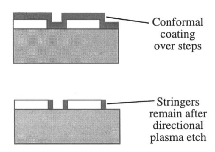
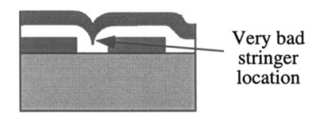
Fig 3.10. - The formation of stringers and the bad results.
#### 3.3.7.2 Chemical Mechanical Polishingchemical mechanical polishing, or CMP: Wafer polishing is a process in which the wafer is pressed against a rotating platen on which an abrasive slurry is provided. Successive dielectric layers are planarized before performing the patterning step of opening vias to permit connection to lower layers. The vias are then filled with metal, after which, the next layer of conductor is deposited and patterned. By using planarized layers, extremely accurate lithography can be performed over complex subsurface topography.
#### 3.3.7.3 Planarization with PolymersSpin-cast polymers tend to planarize substrate topographies. Polyimides are often used for planarization. Because these materials can function at temperatures above 300°C, they can remain as part of the structure. Another polymer that can be used for planarization is the SU-8 resist.
#### 3.3.7.4 Resist EtchbackPlanarization by a polymer can be exploited to planarize an oxide layer over which the polymer is deposited. Photoresist is deposited over oxide topography so as to planarize that topography. Wafer is then plasma etched with an etch recipe that etches the photoresist at about the same rate as the underlying oxide. This results in a much more planar oxide surface.
--- # Chapter 4 Process Integration > Castles in the air - They're so easy to take refuge in. So easy to build, too. >-- Henrik Ibsen, in The Wild Duck